Analysis of a 24- to 30-GHz Phased Array for 5G Applications (Part 1)
Download this article in PDF format.
In 5G communication systems, the phased-array antenna is one of the lead front-end components that defines massive multiple-input, multiple-output (MIMO) performance. The trend outlined in recent years involves providing a robust and complete platform/wizard for RF/microwave engineers to develop more capable antennas and other RF front-end components in less time than before.1 In addition, systems that operate at millimeter-wave (mmWave) frequencies offer benefits that include small antenna sizes and more available bandwidth.2
However, a challenge arises due to the wide variety of application-driven requirements, which encompasses everything from both city and rural environments to realized gain, scan, and polarization performance attributes to impedance matching and more. Such an extensive number of requirements cannot be met by a single and one-time designed element. This means that any practically convenient modeling platform must contain an extensive library of predesigned antenna elements.
Unfortunately, 5G antennas belong to a class of relatively small and densely populated phased arrays in which the total number of radiators typically does not exceed several hundred. If it does, the consistency of results obtained through such system-level platforms ultimately depends on the accuracy of the phased-array element models, which should include the relatively strong mutual coupling with other elements in the array (this mutual coupling can be −15 dB or 0.18 V relative to 1-V element excitation and sometimes even higher).
We will demonstrate that the presence of mutual coupling in such arrays noticeably modifies the input impedance of the elements. This coupling also distorts the shape of the element patterns, resulting in wider and asymmetrical patterns, a splitting of the main beam, a shift in the direction of peak radiation, etc. It’s most alarming that such distortions depend on the radiator position in the array.
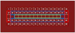
Figure 1 shows a 5 × 16 array in which each of the rim elements marked in red lacks neighboring elements on one side. Each of the next-to-rim elements enclosed in blue rectangles is under the influence of the neighboring rim elements on one side, along with multiple inner elements. Finally, each of the center elements has two layers of neighbors in a symmetrical fashion.
1. This 5- × 16-array panel contains rim elements (red), next-to-rim elements (blue rectangles), and center elements, all of which are influenced by neighboring elements.
Therefore, each of the 38 rim elements plus the 30 next-to-rim elements (85%!) should display unique performance relative to the center elements. Note that even in an array of 32 × 32 = 1024 radiators, the number of such elements is 240, or 23.4%. Therefore, we can expect that an array like the one shown in Figure 1 could be divided into groups of several elements. The individual performance of each element can be determined by its corresponding group.
This analysis demonstrates that arrays of 4 × 4 and higher may be designed based on just three elements. In this case, rows 1 and 5 represent the rim elements along with the outer elements of rows 2, 3, and 4. The inner elements of rows 2 and 4 represent the next-to-rim elements. Lastly, the 12 central elements of row 3 represent the center elements. Therefore, the embedded library database could be truncated without sacrificing the accuracy of the final results.
According to Ref. 3, the power consumption of a 5G station is three times that of its 4G LTE predecessor. In that case, each dBi error in the assessment of array gain can be quite costly.
To date, the antenna-array block of numerous platforms avoids the associated challenges by using data from either a single radiator simulation/test in free space (meaning all elements are identical and mutual coupling is ignored) or a low-complexity and memory-consuming Floquet-Bloch technique. The latter assumes that all radiators are set in an infinite array and are thus identical, since each element is mutually coupled with the same infinite number of driven neighbors. We will demonstrate why both approaches have limited accuracy and how to overcome them.
This two-part article series focuses on several topics. First, mutual coupling and grating lobes are discussed, as they are critical in terms of beamsteering phased arrays. Presented next is the schematic of the broadband patch element appropriate for practical applications.
Afterward, CST Microwave Studio (MWS) (CST MWS is a product of Dassault Systèmes) and MATLAB simulation results (see footnote 1 at the end of the article) are demonstrated—the broadband patch element is placed into the environment of an infinite periodic array. Subsequently, full-wave CST simulation results of a 5- × 16-array based on the same element are presented. The final section discloses the CST analysis results of the same array, but with a triangular lattice.
Mutual Coupling and Grating Lobe in Beamsteering Phased Arrays
Before starting the analysis, note that the total interaction between elements can be loosely divided into three categories: spatial proximity, aperture coupling, and surface-wave interaction. For the most part, the proximity interaction is defined by nearby quasi-static E- and H-fields. For a single microstrip patch radiator, these fields can be seen in Ref. 4 (figures 3 and 4).
The presence of aperture coupling means that some portion of each element’s radiated power is distributed between all other elements in the array behaving as receiving antennas. Hopefully, both types of mutual coupling diminish as the normalized to wavelength inter-spacing between elements increases.
Furthermore, proximity coupling is typically reactive by nature. A substantial amount of this total coupling drops much faster with distance compared to an aperture coupling. The rule of thumb tells us that the array radiators might be considered independent provided that the separation is above a wavelength and the antenna-array structure does not generate and support surface waves. These waves, if they exist, propagate inside the dielectric substrates and mainly stay confined within them, causing undesired coupling that diminishes relatively slowly from element to element. One of the most effective ways to illuminate these waves is to use a thin dielectric substrate of ultra-low permittivity, as we will demonstrate.
The term grating lobes refers to the in-phase addition of a radiated field in more than one direction. Unlike side lobes, the magnitude of the grating lobes might reach the level of the main beam in some unwanted directions.7 In a periodic array, i.e., an array with uniformly spaced and identically excited elements, a single grating lobe appearance is unavoidable when the element spacing exceeds one-half wavelength but is less than one full wavelength.
For example, the pattern of the linear array is free of grating lobes at the shortest designated wavelength, λmin, until:4
where θ is the scan angle and d is the separation between adjacent radiators.
Note that deviations from uniform spacing or the introduction of uncorrelated magnitude/phase error destroy the periodicity of an array and may help to suppress the grating lobe level.9 However, both topics are outside the scope of this article.
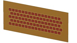
One of the most practical and effective ways to extend the scanning sectors or reduce the level of grating lobes is to change the array schematics. For example, we could move each even row in Figure 1 to the right by a distance equal to half of the array period (Fig. 2). Loosely speaking, in such a so-called triangular lattice, the elements in the odd rows partially fill up the gaps between elements in the even rows and vice versa. The effective separation between array elements then reduces by as much as 16%.9
2. In creating this triangular lattice, each even row in Figure 1 was moved to the right by a distance equal to half of the array period.
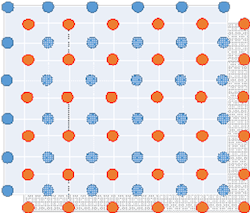
Since the triangular lattice is the superposition of two rectangular shapes (Fig. 3), the grating lobes are not eliminated entirely. Instead, they are diminished in magnitude and shift to higher frequencies or a higher scan angle.
3. The triangular lattice is the superposition of two rectangular shapes.
Array Radiator
To make the outcome of the following comparative analysis relevant for practical applications, a linear polarized (LP), back-fed, stacked U-slot patch radiator optimized for a frequency range of 24 to 30 GHz was chosen (Fig. 4). It’s compact, low profile, easy-to-integrate, lightweight, low cost, and quite simple in terms of providing fast numerical simulations. The combination of two resonant components—a fed patch with a stacked element and a U-slot—results in dual-broadband characteristics5 that are required for 5G systems that must meet the demands for high data rates and low latency.
4. Shown are the element schematics: top view of the fed patch with U-slot (a); top view of the fed and stacked patch (b); and the side view (c).
The side arms of the U-slot are symmetrically positioned with respect to the coax feed point shifted 0.34 mm relative to the origin. The thin dielectric substrate with an ultra-low permittivity of 1.07 (see footnote 2 at the end of the article) ensures the lowest possibility of surface waves. The stacked patch could be supported by a dielectric rod with a small diameter (not shown in the drawing) or an additional layer of the same dielectric. The original cross-section sizes of the radiator substrate and ground plane are 6 × 6 mm, or 0.48λ × 0.48λ at 24 GHz, meaning no grating lobes at any scan angle. However, grating lobes are expected at 30 GHz, as the element inter-spacing grows to 0.6λ × 0.6λ (as will be seen later).
The radiator model was developed using the 3D full-wave CST MWS software and simulated in the time domain to get wideband data over just one simulation run. Afterward, the frequency response is obtained through a fast Fourier transform (FFT). Since the time-domain simulation is performed on a port-by-port basis, it requires less memory and is faster in comparison to a frequency-domain simulation.
A 31- × 31-mm ground plane was added to alleviate the back radiation as well as the ground-edge diffraction.
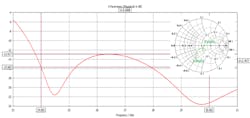
Figure 5 reveals the return loss plot (i.e., 20 × log10(|S11|) over frequency. Excellent wideband performance is demonstrated, as the return loss is below −12 dB at all desired frequencies. Figure 5 also shows a Smith chart, which depicts the corresponding input impedance. As expected, both the return loss plot and the Smith chart indicate the presence of two overlapping resonances—the first at 24.47 GHz and the second one at 29.62 GHz. Thus, the radiator’s performance resembles that of a second-order Chebyshev filter.
5. The return loss and input impedance versus frequency plot reveals excellent wideband performance.
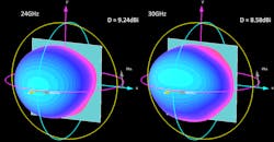
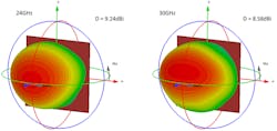
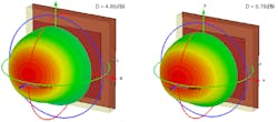
Since the reactive energy stored in E- and H-fields typically reaches extreme levels around resonances,6 this element is expected to have a spike of spatial proximity coupling around these frequencies. Figure 6 depicts 3D element patterns and the associated directivity (dBi) at 24 and 30 GHz.
6. These are the patterns with the extended ground.
Note that the directivity at both frequencies is not directly related to the element’s geometrical size of 6 × 6 mm. Thus, the effective radiation area6 is much broader than the physical area, since the nearby far-field radiation EM fields extend well beyond 6 × 6 mm.
Infinite Periodic Array Environment
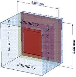
The Floquet-Bloch theory allows one to deduce the property of the whole array with mutual coupling included from a simulation of just a single unit cell (Fig. 7) once certain periodic boundary conditions are established (see blue surface in Figure 7). Behind this approach lies the assumption that all array elements are uniformly excited, identical in behavior, and are placed into the nodes of a planar and uniform grid of infinite extent (i.e., they form an ideal infinite 2D periodic structure).
7. Shown is the element schematic in an infinite-array environment.
While such an approach typically works perfectly well for large arrays of a thousand or more elements, it’s worthwhile to check its applicability for arrays of smaller sizes. The main disadvantage of this approach is that one loses information regarding the element’s active impedance, as well as the level of mutual coupling. The term “active impedance” is defined as the input impedance of some element when only this element in the array is driven, while all others are terminated with matched loads. The remarkable fact is that knowledge of the active impedance is precious, as it allows one to reconstruct the patterns of the driven element and the whole array.8
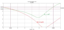
Figure 8 reveals the return loss for two beam positions: boresight (red trace) and θscan = 45° (green trace). Both curves reflect the parameters of every element in the array provided that all elements are driven and demonstrate adequate broadband performance. The comparison of plots in Figures 5 and 6 clearly shows the impact and importance of mutual coupling.
8. Return loss versus frequency is given for two beam positions—boresight (red trace) and θscan = 45° (green trace).
The patterns in Figure 9 are reasonably similar in shape to the ones shown in Figure 6, but the directivities are different. The element directivity is defined by the magnitude and phase distribution of the E-and H-fields not only over the element aperture, but also its vicinity, and could be characterized as so-called effective aperture.6, 7
9. These infinite-array environment patterns are similar to those in Figure 6, but with different directivities.
In the case of a solitary element in free space (Fig. 4, again), the effective aperture exceeds the physical size because the fields cover a larger area than the physical sizes (see Ref. 4, figures 3 and 4). In the case of the element in the infinite array, the effective aperture of the element in Figure 7 is almost equal to its cell, i.e., physical element sizes.
Footnotes
1. At https://emfieldbook.com, readers can find extensive additional information, including ready-to-run CST MWS model files and MATLAB scripts, to extract and process CST simulation data. Click Blog and go to the 5G Broadband Radiator and 5 × 16 Array Thereof section for more results and comments. The raw text files of about 15 GB (3D patterns and complex S-matrix) are available upon request. Just click Contact at the top menu and fill out the message window.
2. For example, ROHACELL 51 IG/A with tan δ = 0.0037 can be formed into a finished core in a mold with all patches directly integrated during the foaming process. See https://www.rohacell.com/sites/lists/re/documentshp/rohacell-dielectric-properties-en.pdf and check out this video:
Vladimir Volman, Ph.D., is a Fellow and PMS of Lockheed Martin (retired) and a consultant.
References
1. David Vye and Jack Browne, “Platform Propels RF Designs from Concepts to Products,” Microwaves & RF, October 2018, pp. 62-63.
2. Jack Browne, “Bringing mmWave Signals to the Masses,” Microwaves & RF, June 2019, pp. 51-54, 68.
3. Sarah Yost, “First to 5G: Who Will Win?” Microwaves & RF, June 2019, pp. 35-36.
4. Kenneth Puglia, “A Brief Tutorial on Microstrip Antennas (Part 1),” Microwaves & RF, November 2018, pp. 40-62.
5. J.A. Anasari and R. B. Ram, “Broadband Stacked U-slot Microstrip Patch Antenna,” Progress In Electromagnetics Research Letters, Vol. 4, pp. 17-24, 2008.
6. Vladimir Volman and Andrzej Jeziorski, Engineering Electrodynamics. House of Maxwell’s Electrodynamics, 2017, see also https://emfieldbook.com.
7. Constantine A. Balanis, Antenna Theory, 3rd Edition, Wiley & Son, 2005.
8. David M. Pozar, “A Relation between the Active Input Impedance and the Active Element Pattern of a Phased Array,” IEEE Transactions on Antennas and Propagation, vol. 51, No. 9, September 2003, pp. 2486-2489, or visit the website: https://pdfs.semanticscholar.org/4f10/5bda3300308e7771276cf65b6557419f2e1d.pdf
9. John S. Williams, ”Electronic Array Design,” Tutorial, visit the website: https://intranet.birmingham.ac.uk/eps/documents/public/emuw2/SCF01.pdf
