Apply a New Approach to Dual-Fed Distributed Amplifier Design
Download this article in PDF format.
The topology of the balanced amplifier1 allows for power to be added at the output. It’s composed of two amplifiers, which may be multistage implementations, placed between the input power divider and the output power combiner (Fig. 1). To enhance the design, a device known as the “Dual-Fed Distributed Amplifier” (DFDA), has been introduced.2
1. The DFDA amplifier configuration includes an input power divider and an output power combiner.
The operating principle of the DFDA involves injecting the signal to be amplified into both ends of the gate line. The output signal is recovered at the two ports of the drain line.
The DFDA is characterized by:2
- A 6-dB increase in gain compared to the conventional distributed amplifier (CDA)3 due to the direct and indirect gains being added. This is not the case with a CDA, in which only the direct gain is taken into account.
- A lower noise factor than that of the CDA due to the absence of the 50-Ω impedance at the ends of the gate and drain lines.
Using two transistors, it’s possible to obtain an open-circuit line at the ends of the gate and drain lines.4 While the gain improves, the bandwidth remains less than that of the CDA.
This article presents a new DFDA design technique that allows for a stable gain over the entire bandwidth. The new amplifier is called a mismatched DFDA (MDFDA). The technique is based on the approximation of the amplifier transducer gain by the Chebyshev polynomial.
Amplifier Design
For this amplifier, the input and output power dividers are replaced by a simple T-piece composed of two 100-Ω transmission lines of unspecified length (Fig. 2). The value of 100 Ω was chosen to match the input with the amplifier’s gate line, as well as the output with the amplifier’s drain line. The values of the components of the gate and the drain line are obtained by approximating the amplifier gain with the Chebyshev polynomial.
2. The T-piece contains two 100-Ω transmission lines.
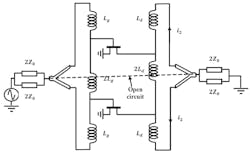
The amplifier diagram of Figure 3 reveals a symmetric plane, meaning that such amplifiers are a product of the association of two identical half-circuits. Thus, the analysis of this type of amplifier will be based on that of a half-circuit.
3. The MDFDA amplifier is symmetric in nature.
The symmetric plane corresponds to an open circuit. Inductances are elements with constants localized; the equivalent diagram of the half-circuit is shown in Figure 4. This diagram is equivalent to that of the single-stage distributed amplifier (SSDA)5 except that the source and load impedance values are doubled (2ZO = 100 Ω).
To express the amplifier’s transducer gain, we use the simple unilateral model of the MESFET transistor, shown inside the dashed line in Figure 4.
4. Shown is the equivalent MDFDA half-circuit.
Here, Cg and Cd are the gate and drain capacitances, respectively, of the field-effect transistor (FET) in common-source mode, while gm is the transconductance. For this structure, the transducer gain, GT, is:
where V2 and i2 are the output voltage and current, respectively.
The transducer gain then becomes:
where x = ω/ωc1 is the normalized frequency with respect to the cutoff frequency of the gate line. The other variables are defined as:
and
Zc1 and Zc2 are the characteristic impedances at relatively low frequencies of the K-constant circuits constituting the gate and drain lines, respectively. They are defined as:
The cutoff pulsation of the drain line is:
We can then get the following results:
where:
The approximation by the Chebyshev polynomial will be applied to the denominator of Equation 3.2. This approximation consists of writing the denominator of gT in the D = 1 + Qn(x) form, or:
Here, ε2 = ε’2 / 1 – ε’2 represents the ripple ratio. We then carry out the approximation by using the Chebyshev polynomial of Tn2(x) of one part of the denominator as follows:
Therefore:
As Qn(x) is of the eighth degree, Tn2(x) must also be:6
After identification, Equations 3 and 7 imply the following set of equations:
where Ai (i = 2, 4, 6, 8) are the coefficients given by Equation 3.3.
Therefore, to design the MDFDA implementation, we must initially solve for the equations shown in the Equation 8 set, in which the roots are α1, α2, α, and ε’. The values taken by these roots are the same regardless of the characteristics of the FET used.
The resolution of equations in the Equation 8 set leads to the following result:
With the values of Equation 9 and by taking ZO = 50 Ω, the design parameters as a function of the gate capacitance, Cg, can be derived as:
We then just need to know the value of Cg to proceed to the design of the amplifier.
The results given by Equations 9 and 10 are general and can thus be applied to any FET. Therefore, it’s sufficient to only know the value of Cgs to proceed to the amplifier design.
Several points can be noted from the obtained results. The FETs with a value of Cd/Cg of less than 0.13 require a shunt capacitor to be added to the drain. The added capacitors combine with Cd to form a new capacitor, Cd’, such that Cd’/Cg = 0.13. The shunt capacitor at the gate should be avoided, since it leads to a reduction of the bandwidth.
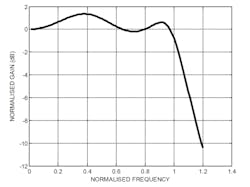
We can update the Equation 3.3 set and then Equation 3.2 with the values given in Equation 9 to calculate the normalized power gain as a function of the normalized frequency for the MDFDA amplifier. Figure 5 reveals the calculated gain. The main characteristic is that this curve is universal. It should be noted that the MDFDA amplifier with a gain that’s approximated by the Chebyshev polynomial achieves a stable gain over a large bandwidth. Here, the bandwidth is defined as a band of frequencies in which the gain is constant or has small variations.
5. Shown is the MDFDA’s normalized power gain as a function of the normalized frequency.
Design and Simulation
We now will carry out the design and simulation of the amplifier studied previously. The internal parameters of the selected transistor are Cgs = 0.17 pF, Cds = 0.006 pF, and gm = 32 mS. The substrate chosen for the microstrip lines is characterized by its relative permittivity, εr, of 10.2. The height of the dielectric and the conductor thickness are 0.25 mm and 17 µm, respectively.
The TXLINE program within the Microwave Office design software was used to calculate the dimensions of the 100-Ω lines of the T-piece. Microwave Office software was used to perform all simulations.
The calculation of the widths (W) of the 100-Ω lines of the T-piece produced a value of 20.129 µm.
Using the equations shown in the Equation 10 set, we determine that Lg = 1210.4 pH, Ld = 2626.16 pH, and Cd = 0.0224 pF. The shunt capacitor with the addition of Cds is:
The transducer gains of the MDFDA were simulated with Microwave Office. The results are provided later in the article.
Using the Real Transistor Equivalent Circuit
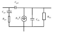
The study here assumed a unilateral transistor with an almost infinite capacitive output impedance value over the bandwidth considered. However, a real transistor does not achieve such characteristics. Figure 6 shows an equivalent circuit of a real transistor. Here, Cgd = 0.016 pF, Rds = 560 Ω, and Rgs = 0.53 Ω.
6. This is the equivalent circuit of a real transistor.
The circuit that’s best suited for this study is the cascode circuit, in which an inductance is added between two transistors to reduce the effects of the input and output capacitances of the first and the second transistors, respectively, at high frequencies (Fig. 7). Figure 8 shows the equivalent circuit of the cascode circuit.
7. The cascode circuit contains an inductance between the transistors.
8. This circuit represents the equivalent of the cascode circuit.
Ref. 5 reveals that, unlike a single-transistor circuit, the cascode implementation is a practically unilateral circuit that achieves an almost infinite output impedance. Thus, to design the MDFDA, we just need to replace the transistors in Figure 3 with cascode circuits.
The shunt capacitor added at the output of the cascode circuit is equal to 0.006 pF. This is because we have the capacitor Cgd of the second transistor at the output of the cascode circuit. The value of the shunt capacitor is then calculated as:
The value of the inductance (400 pH) between the two transistors of the cascode is obtained via optimization.
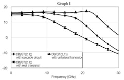
Figure 9 shows the simulated gains of the MDFDA using a unilateral transistor, a real transistor, and the cascode circuit. With a unilateral transistor, we can see that the gain is stable over the entire bandwidth. However, in reality, transistors are not unilateral, causing the gain and the bandwidth to decrease when using a real transistor versus a unilateral one. With the cascode circuit, we obtain good results—the gain of the amplifier is almost the same as the amplifier that employs a unilateral transistor.
9. Shown are the simulated gains of the MDFDA using a unilateral transistor, a real transistor, and the cascode circuit.
Conclusion
This new design approach for the DFDA can apply to any MESFET transistor. The technique makes it possible to maintain a stable gain over a large frequency range due to the approximation of the amplifier gain by the Chebyshev polynomial. The design parameters can be determined in a very simple manner—one only needs to know the gate capacitance of the transistor. This approach allows for a distributed amplifier with substantial gain over a broad bandwidth.
Faycal Amrani is part of the Laboratory of Instrumentation (LINS), electronic and computer science faculty, University of Sciences and Technologies Houari Boumedien (USTHB), Bab Ezzouar, Algiers, Algeria, and M. Trabelsi is in the Department of Electrical and Electronic Engineering, Telecommunication Laboratory of ENP, Algiers.
References
1. Kurakowa. K, “Design theory of balanced transistor amplifiers,” Bell System Technical Journal, 44 (1965), 1675–1698.
2. Aitchison, C. S., et al., “The Dual-Fed Distributed Amplifier,” IEEE MTT-S Digest, 1988, pp. 911–914.
3. Thomas T. Y. Wong “Fundamentals of distributed amplification,” Illinois Institute of Technology, Artech House, 1993.
4. Moazzam, M. R., and C. S. Aitchison, “A High Gain Dual-Fed Single Stage Distributed Amplifier,” IEEE MTT-S Digest, 1994, pp. 1409–1412.
5. F. Amrani, M. Trabelsi, R. Aksas, and M. Azrar, "Bandwidth Improvement of a Single-stage Distributed Amplifier," Microwave Journal, Vol. 53, No. 5, May 2010. pp. 112-122.
6. Jia-Sheng Hong and M. J. Lancaster, Microstrip Filters for RF/Microwave Applications. John Wiley & Sons Inc., 2001.
