UWB Antenna Adds Two Notches
Compact antennas are needed for unlicensed ultrawideband (UWB) applications from 3.1 to 10.6 GHz. For efficient and effective operation with other signals within that band, an UWB antenna has been developed with two frequency notches—one each for the frequencies of WiMAX and wireless-local-area-network (WLAN) systems—for simple coexistence without additional filters.
A number of antennas have been developed in small substrate areas, with microstrip or coplanar-waveguide (CPW) feeds or combinations of technologies.1-4 The UWB frequency span also includes numerous narrowband services, including WiMAX and wireless local area networks (WLANs), which may interfere with UWB operator (or it with them). Such interference can be suppressed by using a spatial filter—such as a frequency-selective surface—above the UWB antenna, although this adds to the cost and complexity.5 Another approach is through the use of an antenna capable of filtering WiMAX signals from 3.3 to 3.8 GHz and WLAN signals from 5.150 to 5.825 GHz.
Band-notched antennas can be designed in various ways, including by using an isolated slit inside a patch, two open-end slits at the top edge of a T-stub, two parasitic strips,6 an embedded semicircular annular parasitic strip,7 and a semicircular slot inside an elliptical slot.8 The antenna structure proposed by Lin and Hung6is simple, featuring compact aperture size. But while it achieves a broad impedance bandwidth with stable radiation patterns, it requires a large ground plane. Moreover, each of these design approaches can notch only one frequency band. Other ways to design band-notched antennas include by embedding various thin slots on the antenna surface, including U-shaped,9 L-shaped,10 square-shaped,11 pi-shaped,12 T-shaped,13 ractal,14 annular, and H-shaped slots.15 It can also be accomplished by adding either a split-ring resonator (SRR)16 or by using a multiresonator load in the antenna structure.17 Unfortunately, all of these approaches add to the complexity of the antenna structure, as well as the fabrication costs.
The proposed compact planar UWB antenna is a possible solution. For improved bandwidth, the top edge of its partial ground plane is modified by introducing triangular shape slots to form a symmetrical sawtooth shape.18,19 The dual band-notched characteristics are achieved by inserting one e-shaped parasitic element and one c-shaped parasitic element on the back side of the patch. The antenna has a simpler design than the other approaches and can be fabricated on low-cost FR4 circuit-board substrate.
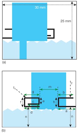
Figure 1 shows the geometry of the proposed UWB antenna. It was fabricated on 1.6-mm-thick FR4 substrate with relative permittivity of 4.6 and loss tangent of 0.02. The antenna consists of a rectangular radiating patch measuring 14.5 x 14.75 mm and a partial ground plane. The partial ground plane is modified by cutting slots on its top edge to form a symmetrical sawtooth shape to enhance the impedance bandwidth. The radiating patch and a microstrip feed line are printed on the front side of a 30 x 25 mm FR4 substrate, while the modified ground plane is printed on the back side. The length and width of the feed line are fixed at 7.25 and 3.0 mm, respectively, to achieve a 50-Ω characteristic impedance. The feed line is terminated in an SMA connector.
1. These diagrams show the geometry of the dual-notched antenna: (a) top view and (b) bottom view.
To achieve the two notches, an E-shaped parasitic element and a C-shaped parasitic element have been etched on the back side of the substrate as shown in Fig. 1(b). The total lengths of the parasitic elements are l1(c + e + g + f + d) and l2(a + h + b), respectively. The thicknesses of the two parasitic elements are t1 and t2 (in mm), respectively, and separated by a distance m. The widths are f for the e-shaped element and h for the C-shaped element. Both elements are a distance n (in mm) above the bottom edge of the substrate. At the notch frequencies, the current flow is stronger around the parasitic elements, with the current paths directed between the different arms of the parasitic elements. As a result, the radiating fields cancel at these frequencies and the antennas do not radiate in these frequency ranges, producing the two notches.
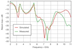
The performance of the UWB antenna was simulated with the IE3D full-wave electromagnetic (EM) simulator from Zeland. The final design was optimized with the following parameters: a = 7.5 mm, b = 6.5 mm, c = 5 mm, d = 6.5 mm, e = 3 mm, f = 4 mm, g = 6.5 mm, h = 4 mm, t1 = t2 = 0.5 mm, and n = 14 mm. For experimental verification, a prototype was fabricated on FR4 and characterized on a model E8362C vector network analyzer (VNA) from Agilent Technologies. Figure 2 shows good agreement between simulated and measured results. The measured impedance bandwidth extends from 2.87 GHz to beyond 11 GHz, with better than 10-dB return loss.
2. These plots compare the simulated and measured return loss for the dual-notched UWB antenna.
The antenna exhibits two notched bands of 3.3 to 3.8 GHz and 5.1 to 5.6 GHz, covering WiMAX and the lower WLAN bands, respectively. In spite of its small size, the antenna covers the full UWB frequency range defined by the United States’ Federal Communications Commission (FCC), with dual-notched bands to minimize interference with WiMAX and WLAN systems. Disparities between measured and simulated results are attributed to manufacturing tolerances and less-than-ideal soldering of the SMA connector on the feed line. Some of these disparities may also be due to the effects of the feed cable used in the measurements, but not included in the simulations.
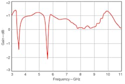
Figure 3 shows maximum antenna gain across the full operating band; the gain drops dramatically at both notched bands. However, the gain also decreases slightly from 8 to 9 GHz, because of the poor impedance match in that band. In spite of the high loss tangent (0.02) of the FR4 substrate, the antenna exhibits good gain, with less than 1-dB variation across the UWB frequency range (except for the two notched bands).
3. The antenna’s peak gain is plotted across its full operating-frequency range.
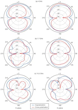
Figure 4 provides E-and H-plane radiation patterns for the antenna at 4.0, 7.7, and 10.2 GHz. The plots, which show bidirectional radiation patterns, indicate that the antenna has a main beam in the broadside direction. At lower frequencies, the E- and H-plane patterns are about the same as a monopole. As the frequency increases, higher-order current modes are excited and the radiation patterns become slightly directional, with the main-beam tilt away from the broadside direction. Still, the antenna exhibits stable radiation patterns over the operating frequency range.
4. These plots show the E- and H-plane responses of the antenna at (a) 4.0 GHz, (b) 7.7 GHz, and (c) 10.2 GHz.
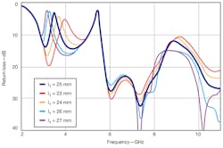
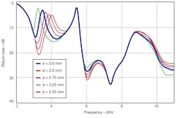
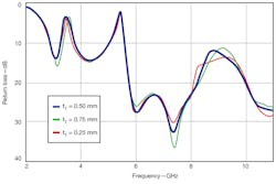
A parametric study was performed to investigate the effects of parasitic elements on the antenna’s dual notches, and IE3D was employed as part of the design and optimization process for the antenna. Since the E- and C-shaped parasitic elements were the main factors in achieving the notches, parameters l1, e, t1}, l2, h, and t2 were used for a sensitivity study. The effects of varying these parameters on the antenna’s band-notched characteristics are shown in Figs. 5 through 10, respectively.
Figure 5 shows simulated return loss for different values of E-shaped element length, l1, with the other parameters remaining constant. As l1 increases from 23 to 27 mm, the center frequency of the first notched band shifts towards higher frequencies; at the same time, the center frequency of the second notched band (for WLAN) remains constant at 5.5 GHz. The bandwidth of the first notched band decreases with increasing l1, indicating that the first notch bandwidth is strongly dependent on the value of l1.
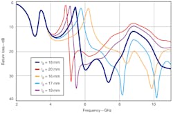
5. These curves show simulated return loss for different values of l1.
Figure 6 shows simulated return losses for different values of e while the other parameters are kept constant. As the value of e increases, the center frequency of the first notched band decreases while the center frequency of the second notched band remains unchanged. The bandwidth of the first notched frequency band is strongly affected by e and decreases with increasing e.
6. These curves show simulated return loss for different values of e.
Figure 7 shows that changes in t1 have little effect on the first notched band and no effect on the second notched band. From these results, it can be concluded that the e-shaped parasitic element affects the first notch band but not the second notched band. In addition, the center frequency and bandwidth of the first notched band are adjusted mainly through the selection of values for l1 and e.
7. These curves show simulated return loss for different values of t1.
Figure 8 shows simulated return-loss curve for different values of l2, the total length of the c-shaped parasitic element. As l2 increases from 16 to 20 mm, the center frequency of the second (WLAN) notched band shifts from 6.2 to 4.9 GHz.The bandwidth of the second notched band also decreases with decreasing l2, while the bandwidth of the first notch band remains unchanged.
8. These curves show simulated antenna return loss for different values of l2.
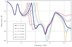
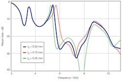
Figure 9 shows simulated antenna return loss for different values of h. For h = 2, 3, 4, 5, and 6 mm, and other dimensions fixed at optimum values, the center frequency of the second notched band moves toward lower frequencies. Changes in h have no effect on the first notched band. Figure 10 shows that the center frequency and bandwidth of the second notched band increases with increasing value of t2, although changes in t2 have no impact on the first notched band. From Figs. 5 through 10, it can be concluded that the antenna’s first notched band (for WiMAX) is controlled by the E-shaped parasitic element, even though that element has no effect on the second notched band. And the second notched band is controlled by the C-shaped parasitic element, which has no influence on the first notched band. By carefully adjusting both parasitic elements, the antenna’s notches can be properly tuned for the WiMAX and WLAN bands, respectively.
9. These curves show simulated antenna return loss for different values of h.
10. These curves show simulated antenna return loss for different values of t2.
Acknowledgment
The authors wish to thank the Ministry of Higher Education, Malaysia, for partially sponsoring this project. This work was supported in part by a grant from Ministry of Science Technology and Innovation, Malaysia.
Rezaul Azim, Doctor
Mohammad Tariqul Islam, Professor
J.S. Mandeep, Associate Professor
Norbahiah Misran, ProfessorInstitute of Space Science (ANGKASA), Universiti Kebangsaan Malaysia, 43600 UKM Bangi, Malaysia; e-mail: [email protected].
Ahmed Toaha Mobashsher, PhD Candidate
School of Information Technology and Electrical Engineering, The University of Queensland, Brisbane St. Lucia, QLD 4072, Australia; e-mail: [email protected].
References
1. R. Azim, M.T. Islam, and N. Misran, “Compact tapered shape slot antenna for UWB applications,” IEEE Antennas & Wireless Propagation Letters, Vol. 10, pp. 1190-1193, 2011.
2. L. Liu, S.W. Cheung, R. Azim, and M.T. Islam, “A compact circular-ring antenna for ultra-wideband applications,” Microwave & Optical Technology Letters, Vol. 53, No. 10, pp. 2283-2288, 2011.
3. R. Azim, M.T. Islam, and N. Misran, “A Planar Monopole Antenna for UWB Applications,” International Review of Electrical Engineering, Vol. 5, No. 4, pp. 1848-1852, 2010.
4. M.T. Islam, A.T. Mobashsher, and N. Misran, “Coplanar waveguide fed printed antenna with compact size for broadband wireless applications,” Journal of Infrared, Millimeter-wave and Terahertz Waves, Vol. 31, pp. 1427–1437, 2010.
5. J. Yeo and R. Mittra, “A novel wideband antenna package design with a compact spatial notch filter for wireless applications,” Microwave & Optical Technology Letters, Vol. 35, No. 6, pp. 455-460, 2002.
6. Y.C. Lin and K.J. Hung, “Compact ultrawideband rectangular aperture antenna and band-notched designs,” IEEE Transactions on Antennas & Propagation, Vol. 54, No. 11, pp. 3075-3081, 2006.
7. C.Y. Hong, C. W. Ling, I.Y. Tarnand, and S.J. Chung, “Design of a planar ultrawideband antenna with a new band-Notch structure,” IEEE Transactions on Antennas & Propagation, Vol. 55, No. 12, pp. 3391-3396, 2007.
8. R. Azim, M.T. Islam, J.S. Mandeep, and A.T. Mobashsher, “A planar circular ring ultrawideband antenna with dual band-notched characteristics,” Journal of Electromagnetic Waves and Applications, Vol. 26, Nos. 14-15, 2012, pp. 2022-2032.
9. H.J. Zhou, B.H. Sun, Q.Z. Liu, and J.Y. Deng, “Implementation and investigation of U-shaped aperture UWB antenna with dual band notched characteristics,” Electronics Letters, Vol. 44, No. 24, pp. 1387-1388, 2008.
10. R. Zaker, C. Ghobadi, and J. Nourinia, “Bandwidth enhancement of novel compact single and dual band-notched printed monopole antenna with a pair of L-shaped slots,” IEEE Transactions on Antennas & Propagation, Vol. 57, No. 12, pp. 3978-3983, 2009.
11. S. Hu, H. Chen, C.L. Law, Z. Shen, L. Zui, W. Zhang, and W. Dou, “Backscattering cross section of ultrawideband antennas,” IEEE Antennas & Wireless Propagation Letters, Vol. 6, pp. 70-73, 2007.
12. Y.L. Zhao, Y.C. Jiao, G. Zhao, L. Zhang, Y. Song, and Z.B. Wong, “Compact planar monopole UWB antenna with band-notched characteristic,” Microwave & Optical Technology Letters, Vol. 50, No. 10, pp. 2656–2658, 2008.
13. M. Ojaroudi, C. Ghobadi, and J. Nourinia, “Small square monopole antenna with inverted T-shaped notch in the ground plane for UWB application,” IEEE Antennas & Wireless Propagation Letters, Vol. 8, pp. 728–731, 2009.
14. W.J. Lui, C.H. Cheng, and H.B. Zhu, “Compact frequency notched Ultra-wideband fractal printed slot antenna,” IEEE Microwave & Wireless Components Letters, Vol. 16, No. 4, pp. 224-226, 2006.
15. J.Y. Deng, Y.Z. Yin, S.G. Zhou, and Q.Z. Liu, “Compact ultra-wideband antenna with tri-band notched characteristic,” Electronics Letters, Vol. 44, No. 21, pp. 1231-1233, 2008.
16. J. Kim, C.S. Cho and J.W. Lee, “5.2 GHz notched ultra-wideband antenna using slot-type SRR,” Electronics Letters, Vol. 42, No. 6, pp. 315-316, 2006.
17. T.G. Ma, R.C. Hua, and C.F. Chou, “Design of a multiresonator loaded band-rejected ultrawideband planar monopole antenna with controllable notched bandwidth,” IEEE Transactions on Antennas & Propagation, Vol. 56, No. 9, pp. 2875-2883, 2008.
18. R. Azim, M.T. Islam, and N. Misran, “Ground modified double-sided printed compact UWB antenna,” Electronics Letters, Vol. 47, No. 1, pp. 9-11, 2011.
19. R. Azim, M.T. Islam, and N. Misran, “Design of a planar UWB antenna with new band enhancement Technique,” ACES Journal, Vol. 26, No. 10, pp. 856-862, 2011.
