Reaching Beyond 100 GHz With Coaxial Connectors
This file type includes high resolution graphics and schematics when applicable.
Coaxial connectors continue to move higher in frequency, with ever-smaller dimensions, driven in part by the development of test equipment such as vector network analyzers (VNAs) for higher-frequency use. But designing reliable higher-frequency coaxial connectors is more than simply a matter of shrinking connector dimensions and developing novel connector interfaces. Connectors reaching towards higher millimeter-wave frequencies have been helped by VNA advances, but also by solid mechanical design of shrinking connector components—to the point where coaxial VNA testing at 100 GHz and beyond is becoming almost trivial.
As coaxial connectors have risen in frequency, they have historically relied on two approaches to mating center conductors: hermaphroditic contact and male-pin/slotted-female contact. The non-sexed approach offered many advantages, the main one being that only one type of connector was required. As frequencies increased, these connectors were made smaller to remain in single-mode operation.
The success of the SMA connector essentially foretold the end of non-sexed connectors. As connectors became smaller for higher-frequency use, it became difficult to make butt-type connectors—pin depth tolerances were critical and the smaller sizes made it difficult to achieve a resilient contact. Such factors would raise the cost of the connectors well above the simple male pin/slotted female contact.
The male/female contact approach became the standard for connectors at higher frequencies. For metrology applications, a slot-less female design was introduced, but it became impractical following the 50-GHz 2.4-mm connector. Slotted connectors are not without problems, however. Designs such as the SMA connector and its two-slot female contact are inexpensive to produce, but easy to damage. A half-round feature is not very flexible, and the SMA connector was initially rated for a lifetime of only 500 connections. SMA designs with a long male pin, which allowed the center conductors to engage before the outer conductors aligned the connectors, meant that careless mating would damage the female contact.
A four-slot contact is much more resilient, such as those used in 3.5-mm connectors designed for compatibility with SMA connectors. With their air-interface design, these precision connectors were needed for calibrated VNA use, but they had their own problems. For SMA compatibility, the size of the male pin was set at 0.914 mm (0.036 in.). The 3.5-mm connector center conductor diameter is 1.52 mm (0.060 in.), which creates two problems.
First, the wall thickness of the female fingers is 0.3 mm (0.012 in.), which is quite thick for such a small-diameter contact. After slotting, the fingers are closed and the part is heat treated. If closed by too little, the contact will be unreliable. If closed by even slightly too much, the insertion force required to mate the connectors will become quite high.
Such high force introduces excess wear and may ever distort the support beads holding the center conductors in place. The large wall thickness of the 3.5-mm connector introduced more pin gap reflection. The impedance of the gap section is 80 Ω. The higher-impedance line section created by the exposed male pin also yields pin gap reflections.
The 40-GHz 2.92-mm K connector, introduced around 1985, minimized many of these problems. A short male pin ensured that, before center conductors could engage, the outer conductor parts aligned the two connectors so the male pin could not damage the female section by being inserted at an angle. The center-conductor diameter of the K connector was designed as 1.27 mm (0.050 in.), leading to a finger wall thickness of 0.18 mm (0.007 in.). This meant that the fingers were more flexible and the insertion pressure was greatly reduced. As a result, K connectors were rated for 4000 connections.
The 50-GHz 2.4-mm connector and the 65-GHz 1.85-mm connector interfaces were introduced by Agilent Technologies. Launch of the firm’s coaxial 50-GHz VNA required the development of the 2.4-GHz connector interface in support of millimeter-wave frequencies.
The 1.85-mm V connector was introduced in support of a coaxial 60-GHz VNA by Anritsu/Wiltron Co. Improvements in V connector bead design made it possible for coaxial VNA frequency coverage to rise first to 65 GHz, then to 67 GHz, and then to 70 GHz. A 110-GHz 1-mm connector was introduced by Agilent, followed by a 110-GHz W connector from Anritsu with the introduction of their 110-GHz coaxial VNA. In development of a 70-kHz-to-145-GHz coaxial VNA system, Anritsu has presented a 0.8-mm coaxial connector.
As connector dimensions shrink, however, they also become more fragile. The thinner wall designs of the K-band and V-band connectors yielded connectors at 1 mm and smaller with female contacts that were too fragile; thus, thicker walls were required. But thicker walls raise the pin gap impedance. Still, it was preferable to a fragile female contact with very thin walls. These connectors are quite expensive and a distorted contact is very undesirable.
Finding machine tools to produce such connectors becomes a challenge, although small drills are available—as small as 0.05-mm diameter. Drills are required to make the holes in the support beads. In addition, a fine saw is needed to cut slots in the female center conductor, with the capacity to cut deep enough to make long enough slots. The finest-dimensioned saw is 0.05 mm (even a 0.025-mm saw was available); the resulting slotted female contact would be very fragile. With a thin-walled design, the insertion force would be very slight, as would be the contact pressure. With a thick-walled connector design, the contact pressure would be greater but the finger flexibility would be slight.
This file type includes high resolution graphics and schematics when applicable.
Design Options
This file type includes high resolution graphics and schematics when applicable.
Higher-frequency connector design options include making the female contact wall very thin, with no slots. The male pin could therefore be large, close in size to the main center conductor. Such a pin could be machined with a 0.05-mm slot. It would employ a slotted portion within an unslotted hole, which would be robust, with no tendency to spread out like the standard slotted female contact. The impedance of this pin gap is 65 Ω, much lower than the lower frequency designs. This makes the connector less sensitive to pin depth reflections.
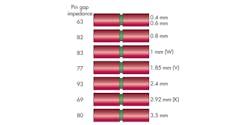
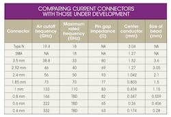
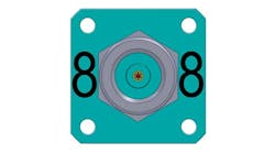
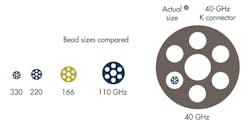
Figure 1 shows different connector dimensions, while the table provides further details on existing and experimental connectors. These experimental 0.6- and 0.4-mm connector designs employ this new slotted male “lobster claw” contact approach. The outer parts of these smaller connectors use dimensions similar to 1-mm connectors to ease handling. But they are also designed so that they cannot be destructively connected—that is, a male connector of a larger size cannot be mated with a female connector of a smaller size. The connectors are identified by a laser-engraved number that shows the connector size (Fig. 2). The number is also etched on the coupling nuts, which have grooves in them that also identify the type.
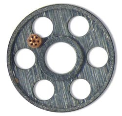
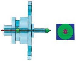
Connectors at frequencies above that of the 1-mm connector will be designed with support beads for maximum rated frequency that is the same as the air-dielectric cutoff frequency, Fco. Lower-frequency connectors have support beads that are larger than the air-dielectric outer conductor size, which means they are capable of an Fco that is substantially lower than the air Fco. The cutoff frequency is inversely proportional to the square root of the dielectric constant of the dielectric material between the center conductor and the outer conductor. The new designs have support beads that are substantially smaller than the size of the air outer conductor. They are designed to have an Fco that is the same frequency as the air Fco(Fig. 3).
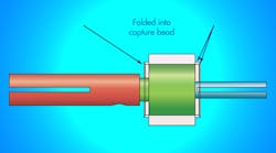
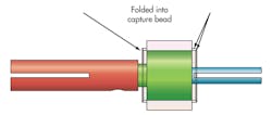
One issue with making the connector bead size smaller than the air dielectric outer conductor size involves how to captivate the bead (Fig. 4). Making a hole in the outer conductor containing the bead presents two problems of its own; First, boring such a small hole deep down in the outer conductor is difficult, and the bead is only held mechanically in one direction. The old designs where the bead is larger than the air outer conductor allowed mechanical capture in both directions. The solution was a sleeve that contained the bead and had an outer diameter about the same size as the air outer conductor (Fig. 5). The sleeves have very thin lips on both ends and are swaged to hold the bead in place. The assembly can then be soldered in place; the beads use high-temperature plastics.
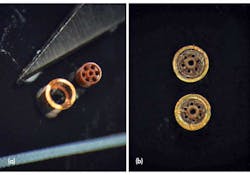
Figure 6 shows a higher-frequency connector, an 0.8-mm assembly that does not use the lobster-claw design. On the left, the bottom is swaged, while the right side shows the assembly after swaging, with the tip of an Xacto blade shown as a size reference. The backside of the connector is a coplanar-waveguide (CPW) design similar to a wafer probe. The center conductor is common, but the outer conductor end cap can be configured to accommodate different CPW designs.
It can be seen how the bead sleeve is soldered into the outer conductor. A connector mates with a component’s internal circuitry by means of its backside interface. This is a critical part of the connector—even more critical at higher frequencies. Substrate traces of 0.1 mm and smaller must be connected repeatably and reliably to these backside interfaces, often with CPW circuitry being used in wafer probes for test systems at higher frequencies. For connectors and components at these higher frequencies, the backside of these connectors is a wafer probe built into the connector.
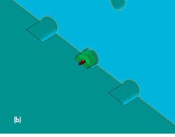
Boring of the outer conductor hole presented the problem related to the difficulty of driving a small boring bar as deep as required. Rather, a drill was used and the transition between sizes was left as a taper. Modeling performed with the High-Frequency Structure Simulator (HFSS) three-dimensional (3D) electromagnetic (EM) simulation software from ANSYS showed that the connector design was less sensitive to tolerance than using a flat bottom created by a boring bar. The center conductor was also tapered and found even less sensitive to tolerance. This design simplification yielded positive RF/microwave performance results.
This file type includes high resolution graphics and schematics when applicable.
Adjustable CPW Interfaces
This file type includes high resolution graphics and schematics when applicable.
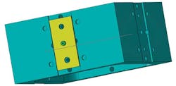
Fortunately, these new connector designs can adjust their backside CPW interfaces, achieving the proper positioning of the connector to the component substrate needed for optimum performance. In this approach (Fig. 7), holes are located at the edge of the flange, centered on the flange edge. A tapered pin allows the flange to be moved up, down, left, and right for proper alignment. When the connector is properly connected to the CPW substrate, the flange screws are tightened (Fig. 8).
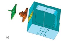
Figure 9 shows a design allowing different front-end connectors to be connected to the housing. It allows wafer probes with different connectors to be attached to a common broadband VNA module. It accepts wafer probes with male and female 0.8- and 1-mm connectors as well as special probes, and can also be used with single-design connectors.
These smaller, higher-frequency connectors may not be used in the traditional manners of lower-frequency connectors, but it is likely they will be used in special system applications and for testing with higher-frequency VNAs. As an example, a currently available Anritsu VectorStar VNA system covers 70 kHz to 125 GHz in one sweep with 1-mm coaxial connectors. The firm has also given a technology demonstration of a 70 kHz to 145 GHz VectorStar system featuring 0.8-mm connectors. Waveguide modules extend that coverage to 1.1 THz. These “lobster-claw” connectors are intended for broadband coverage from 70 kHz to 332 GHz.
As electronic applications reach higher in frequency, coaxial connectors are also extended in frequency. Frequencies once considered the exclusive domain of waveguide are now handled by coaxial connectors. In 1983, for example, a published report (see Microwaves & RF, May 1983, p. 94) offered that a coaxial connector operating as high as 40 GHz in frequency would be unlikely because of mechanical limitations. But connectors almost 10 times that high in frequency are now being designed. As applications reach higher, designers will find ways to extend coaxial connectors to meet those needs.
William W. Oldfield
Anritsu Co., 490 Jarvis Dr., Morgan Hill, CA 85037-2809; (408) 778-2000, FAX: (408) 776-1744
This file type includes high resolution graphics and schematics when applicable.
