Single CDTA Powers Universal Bi-Quad Filter
This file type includes high resolution graphics and schematics when applicable.
Filters come with many responses. Fortunately, a simple design based on a current differencing transconductance amplifier (CDTA) and a few additional passive circuit elements can produce all standard filter functions without significant changes in the basic structure. The filter is well suited for use in integrated-circuit (IC) designs, with natural frequency (ω0) and quality factor (Q) that can both be tuned electronically via changes of CDTA bias current.
Current-mode circuits are gaining attention for analog signal-processing chores—specifically, for their wider bandwidths, larger dynamic ranges, and lower power consumption compared to their voltage-mode counterparts.1 An analog filter is a key building block and is widely used in many fields, such as control systems, measurement, and instrumentation and communication systems. In 2003, D. Biolek proposed the CDTA as a new form of active component.2 It is a really a current-mode device, with two inputs and two outputs all in current form.
In addition, it is equipped with low- and high-impedance input and output terminals, respectively. A CDTA can also adjust the output current gain by means of its bias current. As a consequence, a large number of circuit realizations for current-mode filters using CDTA have been published3-13 Unfortunately, these reported circuits have one or more of the following weaknesses:
The use of more than one active element;
The use of floating resistors;
A lack of high-output impedance ports;
A lack of electronic adjustability; and
An inability to realize completely standard filter functions.
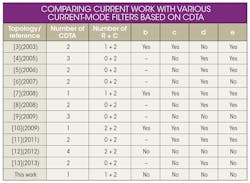
To overcome these weaknesses, a CDTA-based current-mode universal biquad filter with grounded resistor is proposed. This filter contains only one CDTA, one grounded resistor, and two capacitors, and it is appropriate for monolithic integration. The circuit can realize second-order lowpass (LP), bandpass (BP), highpass (HP), bandstop (BS), and all-pass (AP) filter responses. According to the above analysis, a comprehensive comparison of the proposed filter and previously published realizations from refs. 3-13 based on the above-mentioned disadvantages is provided in the table. The new design makes up for all the disadvantages in the best ways among all other filters.
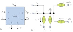
The symbol and equivalent circuit for a CDTA are shown in Figs. 1(a) and (b), respectively. The CDTA’s terminal characteristics can be described by the relationships of Eq. 1:
where p and n are positive and negative current input terminals, respectively; z and x are current output terminals; gm is the transconductance gain; and zz is an external impedance connected to terminal z. According to Eq. 1 and the equivalent circuit of Fig. 1(b), current flowing out of terminal z(iz) is the difference between the input currents through the terminals p and n (ip – in). The voltage at terminal z is transferred to a current at terminal x (ix) through a transconductance gain (gm) which can be electronically adjustable by an external bias current, IB.
Usually this circuit element can be realized with bipolar-junction-transistor (BJT) or CMOS techniques. By way of example, a possible NMOS-based, low-voltage, wide-bandwidth CDTA circuit realization is shown in Fig. 2. It is accomplished through the modification of a low-input-impedance, high-output-impedance current-differencing cascaded transconductance amplifier (CDCTA)14 and the proposed NMOS CDTA can operate with a minimum supply voltage of ±0.8 VDC. The signals pass through only the NMOS transistors, greatly extending the circuit’s bandwidth.
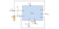
Figure 3 shows the proposed current-mode filter configuration with three inputs and two outputs using a single CDTA. According to Eq. 1 and Fig. 3, a routine circuit analysis of the structure shows that the transfer functions realized by the configuration can be expressed by Eqs. 2-4:
Through the use of Eqs. 2-4, the five filter functions can be achieved as follows:
1. The lowpass response can be realized from Io2 when I1 = I2 = Iin.
2. The bandpass response can be realized from Io1, when I3 = 0 and I1 = I2 = Iin.
3. The highpass response can be realized from Io1, when I1 = Iin and I2 = I3 = 0.
4. The bandstop response can be realized from Io1, when I1 = I2 = I3 = Iin.
5. The all-pass response can be realized from Io1, when I3 = Iin and I1 = I2 = 2Iin.
With a single CDTA, this simple filter can obtain all five filter functions at its high output impedance terminals.
This file type includes high resolution graphics and schematics when applicable.
A Closer Look
This file type includes high resolution graphics and schematics when applicable.
Equations 5 and 6 can be used to find the natural frequency (ωo) and Q of the proposed filter:
while the filter’s bandwidth (BW) can be described by Eq. 7:
From Eqs. 5 and 6, it can be seen that ω1 and Q for the proposed filter are electronically adjustable by means of the bias current to the CDTA. Also, as can be seen from Eqs. 5 and 7, ωo, the natural frequency of the filter, can be independently tuned by varying gm through the bias current, IB, without affecting the bandwidth (BW).
For a look at realistic applications, the performance of the presented circuit may deviate from the ideal by the nonideal characteristics of the CDTA being used. These characteristics are detailed in terms of tracking errors and parasitic impedances, respectively. For analysis of transfer errors, the terminal relations of the CDTA described in Eq. 1 can be further described in Eq. 8:
where αp (with αp = 1 – εp, |εp| << 1) denotes the current tracking error from terminals p to z, αn(with αn = 1 – εn, |εn| << 1) denotes the current tracking error from terminals n to z, and β (with βp = 1 – εd, |ε1| << 1) denotes the transconductance inaccuracy factor from the z to the x terminals of the CDTA, respectively. In this case, the configuration of Fig. 3 was reanalyzed, permitting the characteristic transfer functions of the proposed filter to be calculated by Eq. 9:
The mathematical expressions for the filter parameters ω0 and Q are subsequently changed to Eqs. 10 and 11:
The sensitivities of the active and passive elements to ω0 and Q can be seen by applications of Eqs. 12 and 13, respectively:
From Eqs. 10 and 11, it is clear that the tracking errors of the active and passive elements in the filter circuit may cause small deviations of the values of the filter parameters. Additionally, from the above calculations, all the sensitivities of the active and passive elements of the filter with respect to the CDTA tracking errors are less than unity.
To better understand the universal filter design and its capabilities, the biquad filter represented by Fig. 2 was simulated in the PSPICE software simulator from OrCAD using Taiwan Semiconductor Manufacturing Co.’s (TSMC) 0.18-μm silicon CMOS semiconductor process for the circuit of Fig. 2. The aspect ratios (W/L) for the NMOS transistors are W/L = 24 μm/1 μm for M1-M15c and M20-M27c; W/L = 1 μm/0.6 μm for M16-M17; W/L = 32 μm/0.6 μm for M18-M19. The supply voltages of VDD = VSS = +0.8 VDC and external bias currents (Io) were chosen as 30 μA. In this case, the NMOS CDTA provides very low-input and high-output impedances at the p, n, and z terminals (Rp = Rn ≈ 1.62 Ω, Rz = 300 kΩ), respectively, and very high-frequency operation. Passive components with the following values were used: IB = 200 μA; C1 = C2 = 10 pF; and R = 285 Ω.
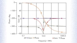
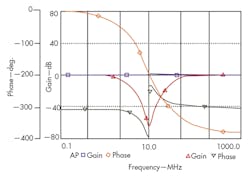
According to Eqs. 5 and 6, this setting has been designed to obtain the LP, BP, HP, BS, and AP filter functions with fo = 10 MHz and Q = 1. Figure 4 shows the simulated responses of the prop2osed filter used as LP, BP, and HP filters. A natural frequency of 9.88 MHz was obtained. Figure 5 shows the simulated frequency responses of the gain and phase characteristics of the BS and AP filters. It is evident from Figs. 4 and 5 that both the natural frequency and the Q are in accordance with the proposed values.
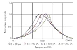
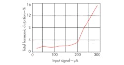
Figure 6 shows simulated a BP filter response when the biasing current, IB, was adjusted with values of 150, 200, 250, and 300 μA, respectively, while maintaining C1 = C2 = 10 pF and R = 285 Ω. The natural frequency and bandwidth of the filter response can be adjusted by means of the CDTA’s input bias current. Figure 7 shows the total harmonic distortion (THD) of the filter, which is less than 3.0% when the input amplitude doesn’t exceed 200 μA.
In short, this CDTA-based current-mode universal biquad filter is relatively simple, with one CDTA, one grounded resistor, and two capacitors, and well suited for monolithic implementations. It can realize all standard biquadratic filter functions and the natural frequency and Q can be controlled electronically by means of the CDTA’s bias current. This filter design is well suited for a wide range of applications, from portable communications products to test equipment.
Acknowledgments
The authors would like to thank the reviewers for valuable comments and helpful suggestions. This work is supported by the National Natural Science Foundation of China (No. 61274020) and the Natural Science Foundation of Hunan Province (No. 14JJ7026) and the Open Fund Project of the Key Laboratory in Hunan University (No. 13K015).
Hairong Lin, Master
Chunhua Wang, Professor
College of Information Science and Engineering, Hunan University, Changsha 410082, People’s Republic of China
This file type includes high resolution graphics and schematics when applicable.
References
This file type includes high resolution graphics and schematics when applicable.
1. C. Toumazou, F.J. Lidgey, and D.G. Haigh, Analogue IC Design: The Current-Mode Approach, Peter Peregrinus, London, 1990.
2. D. Biolek, “CDTA-Building block for current-mode analog signal processing,” Proceedings of the ECCTD’03, Vol. III, Krakow, Poland, 2003, pp. 397-400.
3. D. Biolek and V. Biolková, “Universal biquads using CDTA elements for cascade filter design,” Contribution to the book Computational Methods in Circuits and Systems Applications,” WSEAS Press Electrical and Computer Engineering Series, 2003, p. 232-236.
4. D. Biolek and V. Biolkova, “CDTA-C Current-Mode Universal 2nd-Order Filter,” in Proceedings of the 5th WSEAS International Conference on Applied Informatics and Communications, 2005, pp. 411–414.
5. A. U. Keskin, D. Biolek, E. Hancioglu, and V. Biolkova, “Current-Mode KHN Filter Employing Current Differencing Transconductance Amplifiers,”, International Journal of Electronic Communications (AEÜ), Vol. 60, 2006, pp. 443-446.
6. Tangsrirat W, Dumawipata T, Surakampontorn W. “Multiple-input single-output current-mode multifunction filter using current differencingtransconductance amplifiers”, International Journal of Electronic Communications (AEU), Vol. 61, 2007, pp. 209-214.
7. N.A. Shah, Q. Munazah, and S.Z. Iqbal, “Realization of CDTA Based Current-Mode Universal Filter,” Indian Journal of Pure Applied Physics, Vol. 46, 2008, pp. 283-285.
8. D. Biolek, R. Senani, V. Biolkova, and Z. Kolka, “Active Elements for Analog Signal Processing: Classification, Review, and New Proposals,” Radioengineering, Vol. 17, 2008, pp. 15-32.
9. W. Tangsrirat, “Cascadable Current-Controlled Current-Mode Universal Filters Using CDTAs and Grounded Capacitors,” Journal of Active and Passive Electron Devices, Vol. 4, 2009, pp. 135-145.
10. D. Prasada, D.R. Bhaskara, and A.K. Singh, “Universal Current-Mode Biquad Filter Using Dual Output Current Differencing Transconductance Amplifier,” International Journal of Electronic Communications (AEU);63, 2009, pp. 497-501.
11. F. Kacar and H.H. Kuntman, “A New, Improved CMOS Realization of CDTA and its Filter Applications, “Turkish Journal of Electronic Engineering and Computing Sciences, Vol. 19, 2011, pp. 632–42.
12. M. Kumngern, P. Phatsornsiri, and K. Dejhan, “Four Inputs and One Output Current-Mode Multifunction Filter using CDTAs and All-Grounded Passive Components,” 10th International Conference on ICT and Knowledge Engineering, Vol. 5, 2012, pp. 9-62.
13. J. Jin and C. Wang, “Current-Mode Universal Filter and Quadrature Oscillator Using CDTAs,” Turkish Journal of Electronic Engineering and Computer Sciences, 2013.
14. J. Xu, C. Wang, and J. Jin, “Current Differencing Cascaded Transconductance Amplifier (CDCTA) and Its Applications on Current-mode Nth-order Filters,” Circuits Systems & Signal Processing, 2013, pp. 1-17.
This file type includes high resolution graphics and schematics when applicable.
