Single Microstrip Layer Holds UWB Log-Periodic Antenna
This file type includes high resolution graphics and schematics when applicable.
Microstrip antennas have long been used as reliable components with small profiles, large directional beams, and high gain.1 Unfortunately, they also exhibit narrow impedance bandwidths, with single-layer dielectric-resonator-type patch antennas providing only a few percent of center frequency.2
Microstrip antenna impedance bandwidth can be increased by means of crossfeed logarithmic modes,3,4 where microstrip antennas have been achieved with several octaves of coverage. In addition, through a coplanar feed approach with quarter-wavelength (λ/4) microstrip lines, an impedance bandwidth from about 1.3 to 4.0 GHz has been reached.5
A number of reports6,7 have described the use of various feed approaches—including perforated feeding, aperture coupled feeding, and embedded coplanar feed logarithmic periodic microstrip antennas—for improved impedance bandwidths, with log-period microstrip antennas showing great promise. One problem with log-period microstrip antennas, however, has been the use of a double-layer circuit medium, in which said medium must be perfectly aligned for best performance. This can be difficult to achieve at the design and production stages.
A log-periodic microstrip antenna is a form of traveling-wave antenna. Its terminal portion works with the impedance-matching load to absorb radiated energy and reduce reflected energy. The terminal section is important, since it can greatly improve the antenna’s radiation pattern in the working frequency band. But terminal matching load absorption can significantly reduce the overall efficiency of a microstrip antenna (especially across the upper frequency range), and efficiency loss can reach 10% or more.8
Adding a terminal matching load to a log-periodic microstrip antenna will increase the complexity and cost, and eventually may cause it to fail. The bandwidth of a log-periodic microstrip antenna is determined by periodic factor k and microstrip patch unit number n, with the antenna bandwidth equal to kn - 1. If k is large, the number of required microstrip units is reduced.
For example, for a scale factor of 1.05 or less, at least 21 microstrip units are required for a working bandwidth of 2.6:1. For a scale factor of 1.1, only 11 microstrip units are needed to achieve the same bandwidth.
This file type includes high resolution graphics and schematics when applicable.
Improved Design
This file type includes high resolution graphics and schematics when applicable.
By way of improvement, this article proposes a new type of single-layer log-periodic microstrip antenna. It uses microstrip-line capacitive coupling to feed a coplanar microstrip patch array. The single-layer design provides excellent structural strength and can be fabricated by means of standard single-layer printed-circuit-board (PCB) technology.
The antenna employs a new type of terminal compensation structure for improved efficiency. A large scale factor is used to reduce the number of microstrip patch elements required. A log-period microstrip antenna with 11 patch units was designed, simulated, and fabricated to demonstrate the approach. With a scaling factor of k = 1.1, the antenna obtains a 3.03:1 impedance bandwidth with stable radiation pattern.
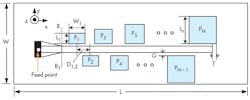
Figure 1 shows the single-layer log-periodic microstrip antenna design. It consists of a 50-Ω to 100-Ω impedance-transformation line, a 100-Ω microstrip feeder, and a set of microstrip coupling feed patches. The antenna was fabricated on 3-mm-thick, glass fiber and Teflon dielectric substrate material with relative permittivity of 2.65. The size of the microstrip patch is based on the log-periodic arrangement presented in Eq. 1:
k = Wi/Wi – 1 = Li/Li – 1 = Di, i + 1/Di, i – 1 (1)
where
Di, i + 1 = the distance from the ith patch to the center of the ith + 1 patch;
Di, i - 1 = the distance from the ith patch to the center of the ith - 1 patch;
Li = the height of the ith patch; and
Wi = the width of the ith patch.
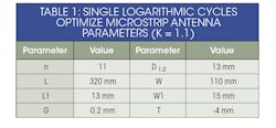
The High Frequency Structure Simulation (HFSS) electromagnetic (EM) simulation software from ANSYS was used for the simulation and optimization of the antenna, with the optimization parameters of Table 1. In using a coplanar coupled microstrip line feed approach, the couple gap, G, is an important parameter that will impact the efficiency of the feed so, it must be carefully considered.
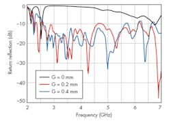
Figure 2 shows simulated reflection coefficients for different values of G; it details the results for reference plane BB1 and does not consider the influence of the impedance transformation structure or the SMA connectors used with the antenna.
The coupling gap G has a strong effect on the antenna impedance matching; when G = 0.2 mm, the antenna impedance matching is at an optimum. When G = 0.4 mm and the frequency is higher than 2.55 GHz, the impedance matching is better since part of the antenna array can absorb the high-frequency energy and radiate the higher-frequency energy, so that reflections are small in the antenna terminal.
For a frequency range of 2.25 to 2.55 GHz, the best matching is achieved with G = 0.2 mm. The distance between the feeder and microstrip patch has a strong effect on the coupling of the log-periodic microstrip antenna, while also impacting the impedance-matching characteristics.
This file type includes high resolution graphics and schematics when applicable.
Compensation Concerns
This file type includes high resolution graphics and schematics when applicable.
Ideally, the feeder should supply energy to the coupled microstrip patches as efficiently as possible across a full frequency band of interest. The microstrip patches are designed to achieve effective energy radiation while reducing feeder terminal reflections. In this way, the feeder can reduce the antenna’s dependence on the terminal matching load and improve antenna efficiency.
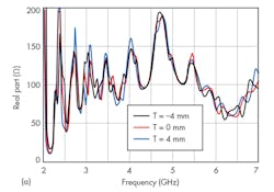
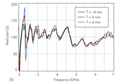
The compensation microstrip line helps improve the efficiency of the log-periodic antenna. The compensation of microstrip line length T can be divided into positive and negative modes. The microstrip line with positive compensation value can be considered as an open-circuit transmission line, equivalent to a series capacitive load without loss. The microstrip line with negative compensation value can be considered as having no inductive load.
The main function of the compensation microstrip line is to provide the antenna’s first resonance point, near 2.36 GHz (Fig. 3). The microstrip line should be chosen for optimum impedance matching. The line is relatively lossless and is used to improve the antenna’s impedance matching in the low-frequency band. The antenna’s terminal energy will be reflected towards the secondary radiation, so the compensation of the microstrip line may influence the directional pattern of the periodic microstrip antenna in the low-frequency band, so it requires further analysis.
By using different matching load terminals and terminal compensation structures, it was possible to see their effects on the microstrip log-periodic antenna design (Table 1). The terminal matching load was simulated via a “lumped resistive-inductive-capacitive (RLC) boundary” approach. Using a size of 22.4 × 3.0 mm, the resistance and characteristic impedance of the microstrip feeder were consistent, at 100 Ω.
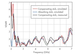
Figure 7 offers a simulation of the antenna voltage standing wave coefficient. Between 2.4 and 6.8 GHz, the standing wave coefficients of the two antennas are similar, with good matching effects.
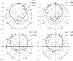
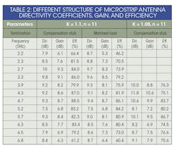
At less than 2.3 GHz, the terminal impedance matching characteristics of the matching load are still good, but all of the microstrip patch units cannot work effectively across this wide band. It can be deduced that the matching load will absorb a great deal of terminal energy, and the overall efficiency of the antenna will not be high at the lower frequencies (Table 2). This is similar to the effects of characteristic impedance matching, and the radiation patterns of the two experimental antennas are very similar at 3.3 GHz (Fig. 4).
At 2.3 GHz, certain differences exist in the x-z plane of the radiation patterns of the two antennas; for the antenna adopting the matching load terminal, the beam width is narrower with a higher directivity. These differences are mainly caused by differences in the terminal impedance matching load and the terminal compensation structures. When the terminal matching load fully absorbs the EM energy, there are no reflections on the antenna terminal, so the radiation pattern remains unaffected.
An effective terminal compensation structure will reflect all energy present at the terminal back to the microstrip patch array for greatly enhanced efficiency. When the matching load terminal antenna directivity is higher, the gain is less than when using a compensation structure in the antenna terminal. This is mainly due because the matching load absorbs a great deal of the terminal energy, and the total antenna efficiency suffers.
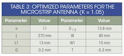
To evaluate the log-periodic microstrip antenna performance with a large periodic factor of k = 1.1, the effects of k on antenna pattern and gain must be understood. Table 3 shows antenna parameters when choosing a smaller scale factor of k = 1.05 as a reference.9 The VSWR of an antenna with k = 1.05 is better than for an antenna with k = 2.5; the simulation impedance bandwidth is from 3.35 to 6.95 GHz, which is consisted with the bandwidth of the antenna impedance with k = 1.1.
Figure 5 presents the radiation pattern of antenna with k = 1.05, which is similar to the pattern for the antenna with k = 1.1 (only the directivity ratio is 0.65 dB higher). This demonstrates that when adopting a larger scale factor k, it is possible to reduce the number of patch elements required in the microstrip antenna, but with some sacrifice in gain performance.9
Figure 6 shows a pair of antennas fabricated by means of a single-layer microstrip PCB process, using the main parameters from Table 1. The impedances of the antennas’ bandwidths were tested using a commercial vector network analyzer (VNA), a model 8722ES from Agilent Technologies [now Keysight Technologies], with the results shown in Fig. 7. The simulated and measured responses are quite close. The impedance bandwidth of the test standing wave ratio is less than 2.5:1 from 2.5 to 6.85 GHz, and reaches 3.03:1.
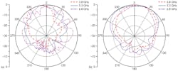
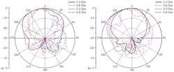
Figure 8 presents the antenna’s radiation pattern as measured in an anechoic chamber, with the test results generally matching the simulation responses. Figure 9 shows additional test and simulation comparisons, with only slight differences. This may be because the gain of the standard horn is about 20 dB higher than the average gain of the test antenna, boosting the calibration error.
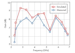
The measured gain is better than 6.5 dB from 2.4 to 6.6 GHz, for a gain-bandwidth product of 2.75:1. The gain fluctuation was consistent between the simulation figures of 2.4 dB and the measured gain fluctuations, within 2.0 dB.
Acknowledgments
The research is partly supported by the National Science Foundation of China (grant Nos. 61271160 and 61172045) and National Fundamental Fund of Personnel Training (grant No. J1103210).
Yanfeng Geng, Researcher
Runbo Ma, Researcher
Baoming Chen, Researcher
Wenmei Zhang, Researcher
Shanxi University, College of Physics and Electronics, 030006 Taiyuan, Shanxi 039996, People’s Republic of China
This file type includes high resolution graphics and schematics when applicable.
References
This file type includes high resolution graphics and schematics when applicable.
1. D.M. Pozar, “Microstrip antennas,” Proceedings of the IEEE, Vol. 80, No. 1, 1992, pp. 79-91.
2. H. Ozeke, S. Hayashi, N. Kikuma, and N. Inagaki, “Quasi-log-periodic microstrip antenna with closely coupled elements,” Electrical Engineering Japan, Vol. 132, No. 2, May 2000, pp. 58-64.
3. P.S. Hall, “New wideband microstrip antenna using log-periodic technique,” Electronics Letters, Vol. 16, No. 4, February 1980, pp. 127-128.
4. P.S. Hall, “Multi-Octave bandwidth Log-Periodic microstrip antenna array,” IEEE Proceedings of Microwave Antennas & Propagation, Part. H, Vol. 133, No. 2, April 1986, pp. 127-136.
5. H. Pues, J. Bogaers, R. Pieck, and A. van de Capelle, “Wideband quasi- log-periodic microstrip antennas,” IEE Proceedings on Microwave Antennas & Propagation, Part H, Vol. 128, No. 3, June 1981, pp. 159-163.
6. X. Chen, W.G. Yeoh, and Y.B. Choi, “A 2.45-GHz near-field RFID system with passive on-chip antenna tags,” IEEE Transactions on Microwave Theory & Techniques, Vol. 56, No. 6, June 2008, pp. 1397-1404.
7. H.K. Smith and P.E. Mayes, “Log-Periodic array of dual-feed microstrip patch antennas,” IEEE Transactions on Antennas & Propagation, Vol. 39, No. 12, November 1991, pp. 1659-1664.
8. J.-Y. Li, “Compact size dipole antenna,” Electronics Letters, Vol. 44, No. 21, October 2008, pp. 1229-1231.
9. R.L. Carrel, “The Design of Log-Periodic Antennas,” IRE International Convention on Receiving, Vol. 1, 1961, pp. 61-75.
This file type includes high resolution graphics and schematics when applicable.


