Picosecond Switching, Plasma Create All-Electronic Terahertz Pulses
This article appeared in Electronic Design and has been published here with permission.
The quest for sources of terahertz-band energy using lasers, electro-optics, solid-state devices, and anything else imaginable continues—no matter how “far out”—as this relatively open frontier of electromagnetic spectrum beckons with its enormous bandwidth, potential for extreme data rates, and other interesting possibilities (such as the ability to “see” below the skin or through walls). Another recent project uses ultra-fast, wide-swing switching with a relatively simple arrangement compared to some of the other approaches.
Researchers in the Power and Wide-band-gap Electronics Research Laboratory (POWERlab) at Ecole polytechnique fédérale de Lausanne (EPFL, Lausanne, Switzerland) have devised, built, and evaluated a chip-based nanodevice that can generate relatively high-power THz signals using picosecond switching. The core of this generator consists of two metal plates set 20 nm apart (Fig. 1).
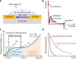
1. The concept of a nanoplasma switch: Schematic of the structure of a nanoplasma switch with gap length g (a). The switch is normally OFF and becomes ON at the threshold voltage V = VTH by electron transport in the high-electric-field region. Current–voltage characteristics of a nanoplasma switch (b). The transition from the insulating phase to the conducting phase is ultra-fast, while the conducting-to-insulating transition is controlled by the external circuit. Threshold voltage VTH versus gap distance, showing a much larger electric field (E) for devices with nanoscale gaps (c). The higher electric field in a shorter gap distance results in a much faster electron transport for nanoplasma devices (d). (Source: EPFL)
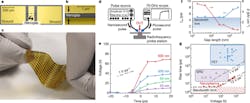
An applied voltage causes electrons to surge toward one of the plates, where they form a nanoplasma. Once the voltage reaches a threshold, the electrons are emitted almost instantly to the second plate. The rapid movement enabled by the fast switching creates a high-intensity pulse that produces high-frequency waves (Fig. 2). Such fast switching and wide voltage slewing of the “spark” is critical. In this arrangement, the voltage transitions from 10 V (or less) to 100 V in the 5- to 10-ps range, and can do so at a rate up to 50 MHz.
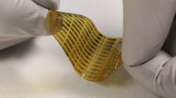
2. Implementation of nanoplasma switches: Micrograph of a nanoplasma switch integrated with radiofrequency pads (a). A scanning electron microscope image of the nanogap (b). Fabricated devices on Kapton showing their possible integration in flexible substrates (c). Schematic of the experimental setup for switching characterization of the nanoplasma devices (d). Measured switching waveforms showing 6-ps rise time of high-amplitude signals (e). Measured switching time (tSW, blue) together with the estimate dielectric field in the nanogap (E, red) (f). After de-embedding the effect of cable and radio-frequency probe, a 5-ps rise time was obtained. Benchmark of the rise time/switching voltage of nanoplasma versus other state-of-the-art electric devices (g). (Source: EPFL)
The researchers note that the switching frequency of this experiment was limited by their solid-state pulse generator. They demonstrated a 20-MHz switching frequency at 390 V together with an ultra-fast recombination time of less than 20 ns, which enabled further increase in the switching frequency up to 50 MHz.
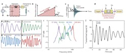
By integrating these devices with a dipole antenna for signal emission, high-power terahertz signals with a power–frequency (Pf2) product of 600 mW-THz2 were emitted, with an average peak power of 50 W at 109 GHz (Fig. 3). The team maintains that their ultra-fast switching speed of better than 10 V per picosecond is about two orders of magnitude larger than that of field-effect transistors and more than 10X faster than that of conventional solid-state switches.
3. Nanoplasma-based millimeter-wave/terahertz source: Circuit diagram of millimeter-wave/terahertz source realized by a nanoplasma switch (a). RS is the series resistance of the voltage source VS. The voltage source VS smoothly charges a fast resonator, which is excited at V = VTH when the nanoplasma switch turns ON with picosecond transition time (b). Illustration of the generated millimeter-wave/terahertz pulse at t = tSW (c). Schematic of the experimental setup; the terahertz pulse is emitted by a transmitter antenna (Tx) connected to the nanoplasma switch and the received wave (Rx) is measured by an ultrahigh-frequency oscilloscope (d). Measured waveforms with bowtie antennas with different sizes (the transmitter and receiver antennas have the same size) resulting in central frequencies of 27 GHz (e), 50 GHz (f), 80 GHz (g) and 109 GHz (h). Frequency spectrum of the received signals for four different antenna sizes showing the flexibility of the method in generating high-frequency signals at different frequencies (i). Calculated radiated signal from the transmitter antenna, based on the measured S21 after de-embedding the effect of the cables and radio-frequency probe, showing a high average peak power of 50 W at 109 GHz (j). (Source: EPFL)
Team leader Prof. Elison Matioli noted that “normally, it’s impossible to achieve high values for both variables [high energy and high frequency]. High-frequency semiconductor devices are nanoscale in size. They can only cope with a few volts before breaking out. High-power devices, meanwhile, are too big and slow to generate terahertz waves. Our solution was to revisit the old field of plasma with state-of-the-art nanoscale fabrication techniques to propose a new device to get around those constraints.” He added that “the new device pushes all the variables to the extreme—high-frequency, high-power, and nanoscale aren't terms you'd normally hear in the same sentence."
This work was partially supported by the Swiss Office of Energy and the Swiss National Science Foundation (SNSF), and is summarized in this two-minute video:
Full details are in their paper “Nanoplasma-enabled picosecond switches for ultrafast electronics” published in Nature (with over one hundred references); it’s behind a subscription paywall but an unlocked version is available here. The locked link also includes unlocked links to extended figures and captions, while the unlocked version contains two more pages on “Methods.”


