This article is part of the TechXchange: Wide-Bandgap Semiconductors.
What you’ll learn:
- The truth about the most popular myths around silicon carbide (SiC).
- How SiC compares to IGBTs.
Looking to use silicon carbide (SiC) in your design? Make sure you don’t get fooled by some of the myths surrounding this technology.
1. SiC is only valuable as a replacement for silicon IGBTs.
In some sectors of the design community, there’s a belief that the only choices when replacing silicon MOSFETs and IGBTs is to use gallium nitride (GaN) for MOSFET replacement and silicon carbide (SiC) to replace IGBTs.
Nothing could be further from the truth. 650-V-rated SiC MOSFETs offer excellent performance, including a very competitive RDS(ON) * Qg figure-of-merit (FOM) and very little reverse-recovery charge. It -s an excellent alternative to silicon MOSFETs in hard-switching apps such as totem-pole power factor correction (TPPFC) or a synchronous boost.
2. SiC has little value in high-frequency applications.
Possibly due to its success in lower-frequency, high-power applications such as electric-vehicle (EV) traction inverters at 10 to 20 kHz, some believe that SiC isn’t well-suited to higher-frequency applications. Thus, GaN should be used for fast switching.
SiC continues to advance rapidly as a technology. Recently, meaningful reductions have been made to the die area, thereby enhancing high-frequency (>100 kHz) operation. As a result, SiC devices are used successfully in applications such as TPPFC at 100 kHz and soft-switching LLC at 200 to 300 kHz.
Emerging technologies such as trench and cascoded SiC MOSFETs will further reduce key FOMs, enhancing performance in high-frequency applications.
3. SiC devices are subject to supply-chain restrictions.
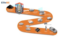
Component availability is an issue in some sectors. However, in other sectors, supply chains have strengthened—e.g., onsemi’s recent acquisition of GTAT. According to onsemi, it’s the only large-scale supplier with end-to-end supply capability, which includes volume SiC boule growth, substrate, epitaxy, device fabrication, best-in-class integrated modules, and discrete package solutions.
To support the anticipated growth in SiC over the next few years, the company plans to increase the capacity of substrate operations fivefold and make substantial investments in doubling device and module capacity across all sites by 2023. That will be followed by nearly doubling capacity again by 2024, with the capability to double capacity in the future.
4. SiC is only suited to high-end niche applications.
This myth seems to be based on SiC being so successful in electric-vehicle (EV) traction inverters. However, the need for increased power density and efficient operation across almost all application sectors means that SiC benefits are widely used in designs such as EV onboard chargers (OBCs), solar photovoltaic (PV) modules and other renewables, as well as cloud computing.
5. SiC doesn’t have a fully developed ecosystem.
One could argue that this is, in fact, true—but only in the sense that there’s constant innovation in all areas of technology. Established technologies such as mixed-signal ICs and microprocessors continue to evolve, decades after their inception.
SiC—and its ecosystem—is evolving rapidly as the technology enters the mainstream. A wide choice of commercially available SiC devices and associated gate drivers are commercially available in numerous packaging styles to suit multiple applications. The knowledge base for SiC is increasing throughout the industry as manufacturers develop their support, including applications engineering teams, reference designs, application notes, and simulation models/tools.
6. SiC FET gate drivers are quite complex
This isn’t true now and has never been true. This seems to stem from early designs where many engineers attempted to drive SiC MOSFETs with drivers intended for silicon MOSFETs /IGBTs, or developed their own complex glue circuitry to drive them.
Today, many dedicated SiC drivers in the market offer convenient features such as negative gate drive, DESAT, OCP, OTP, and other protections. If you select the right driver, driving SiC is no more difficult than driving a silicon MOSFET.
7. SiC requires a negative turn-off gate voltage.
While many designers use a negative turn-off gate voltage to protect SiC devices from “bouncing” or inadvertently turning back on as a result of switching transients, it’s not a strict requirement. In fact, there are many examples of successful SiC designs without a negative gate-voltage drive.
As with all design, good practices should be followed. With SiC MOSFETs, the layout should follow guidelines to minimize parasitic elements and the gate-driver sink current must be high current so that the gate is firmly held off.
8. Junction isolated gate drivers are adequate for all SiC designs.
In a limited number of applications (e.g., TPPFC), it’s technically correct that a junction isolated gate driver might yield acceptable results. However, it’s always worth bearing in mind that galvanically isolated gate drivers offer enhanced noise immunity and handle switch-node dv/dt transients better without any false-tripping.
Because SiC MOSFETs switch rapidly and have lower gate charge (Qg) than equivalent silicon devices, a galvanically isolated gate driver is always considered to be a good choice for a robust design—even in applications where it’s not strictly required.
9. SiC is less robust than silicon IGBTs.
Not true, although making a true “like for like” comparison can be difficult. The wide bandgap (WBG) of SiC material enables better avalanche ruggedness within SiC MOSFETs. That’s because the thermally generated carrier concentration of SiC devices is much smaller than that of silicon devices.
As SiC devices have smaller geometries, their short-circuit withstand time is lower than that of an IGBT. However, using the appropriate SiC gate driver ensures that the short-circuit event is detected and the device is turned off in a reasonable time, thereby ensuring system ruggedness.
10. SiC solutions are too expensive.
A perception remains that SiC solutions are expensive, but this isn’t true if the solution is looked at holistically. If an overly simplistic comparison is made—silicon MOSFET versus equivalent SiC device—then there will be a small price premium for the SiC device.
However, to illustrate the point, we can consider a typical silicon-based 30-kW power solution. Here, 90% of the overall cost is found in the inductors and capacitors (60% and 30%, respectively), with the semiconductor devices representing only 10% of the overall BOM cost.
If the silicon MOSFETs are replaced with SiC switches, then capacitance and inductance size will shrink by 75%, significantly reducing cost (as well as size) and thus outweighing the cost increase in the switching components.
Further, Si solutions tend to offer lower efficiency compared to SiC, and consequently they need expensive and bulky heatsink solutions. As a result, the total BOM cost of a SiC solution has reached a point where it’s lower than a silicon solution.
11. Increasing voltages in EV and solar applications are a problem for SiC.
SiC is excellent for applications within the 650-V space, such as ac-dc power conversion. The battery voltage on many EVs is moving from 400 to 800 V or even 1,000 V, and within solar photovoltaic (PV) systems the input voltage is increasing from 600 to 1,500 V.
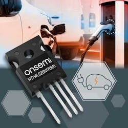
To meet this need for increased breakdown voltages, onsemi developed a range of 1700-V M1 planar EliteSiC MOSFET devices that are optimized for fast switching applications. Alongside the MOSFETs, the company also launched a range of 1700-V SiC Schottky diodes.
Read more articles in the TechXchange: Wide-Bandgap Semiconductors.


