Image

Setting Strategies For Transmission Lines

Oct. 15, 2008
In building a strategy for effective integrated-circuit design, it is important to understand the characteristics of different printed transmission lines.

Last month, the first part of this article made recommendations for choosing the physical dimensions of stripline. A large height, H, ensures high power-handling capability. Smaller H requires a smaller strip for the same impedance, leading to higher losses. The thickness, h, of the suspended stripline dielectric substrate should be as small to minimize losses and parasitic inductance of vias, as well as to reduce cost.

For slotline, the slot width W increases with the characteristic impedance, which becomes less sensitive to substrate height h. For coplanar waveguide, the gap S between printed lines is usually small and supports electric fields primarily concentrated in the dielectric material. To concentrate the fields in the substrate area and to minimize radiation, the dielectric substrate thickness, h, is usually chosen to be about twice the dimension of the slot width.

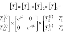
Matrix representations are popular for analysis of transmission lines in RF/microwave applications. An optimization procedure should include analysis of the transmission-line interface. The interface can represent a connection to other transmission lines, to loads, or to different circuit elements or devices. The key parameters associated with the interface include impedance, electrical length, physical dimensions, configuration, and technology process. The most important electrical parameter is transmission-line/interface impedance matching. Figure 9 shows series connections between a transmission line and input/output interface with identical input/output impedances, z. The two-port network can be represented by a cascade arrangement of three two-port networks: input interface block 1 with transfer matrix 1, transmission line 2 with transfer matrix 2, and output interface block 3 with transfer matrix 3. The transfer matrix, , of the three-cascade network is the product of the transfer matrices representing the individual two-port networks2:

where

? = a + i = the transmission-line propagation constant,
a = the attenuation constant,
= the phase-shift constant, and
L = the transmission-line length.

Because matrix multiplication is not commutative, it is necessary to multiply the matrices in the proper order (from source to load in Fig. 9 ). From Eq. 4, it is possible to obtain the scattering matrix coefficient, S11, equal to the input reflection coefficient, Gin :

For the ideal matching condition, S11 = 0, from Eq. 5 it is possible to obtain:

Transmission-line characteristics can be found using Eq. 6 and the known interface performance.

If the interface impedance is different from the transmission line impedance, Fig. 9b represents an equivalent network, where two additional two-port networks with different impedances. The transfer matrix, , of the fivecascade network is the product of the transfer matrices of the two-port networks (Eq. 7), with R1 = z2/z1 and R2 = z3/ z2. For the ideal matching condition S21 = 0 or T21 = 0.

Design tradeoffs for planar transmission lines include cost versus tolerances; cost versus thermal characteristics; cost versus reliability; cost versus loss; cost versus integration index; integration index versus tolerance; size versus Q; size versus tolerance; and size versus maximum power. The most contradictory requirements are size versus loss. Conductor properties and substrate surface roughness should be considered for optimum performance/cost tradeoff.

The factors affecting the choice of substrate thickness are often controversial. On the positive side, the effects of decreasing substrate thickness include compact circuits, ease of integration, the lower likelihood of higher-order radiation modes, and low parasitic inductance for viaholes. But the decrease in substrate thickness, while maintaining a constant characteristic impedance, will be accompanied by a narrowing of the conductor width. The narrower conductor width leads to higher conductor losses and lower Q. For smaller widths and thickness, fabrication tolerances become more severe. Microstrip circuit dimensions usually decrease with increasing dielectric constant, but losses usually increase because higher dielectric constant materials usually have higher loss tangents, and for the same characteristic impedance, reduced conductor line widths have higher ohmic losses.

REFERENCE

4. R. Garg, "The Effect of Tolerances on Microstripline and Slotline Performances," IEEE Transactions on Microwave Theory & Techniques, vol. MTT-26, No. 1, January 1978.
Sponsored Recommendations

MMIC Medium-Power Amplifier Covers 6 to 12 GHz

Nov. 11, 2024
Mini-Circuits is a global leader in the design and manufacturing of RF, IF, and microwave components from DC to 86GHz.

RF Amplifier and Filter Testing with Mini-Circuits Power Sensors

Nov. 11, 2024
RF power sensors are essential for accurately measuring RF components like filters and amplifiers, focusing on parameters such as insertion loss and gain. Employing instruments...

High-Frequency Modules to 110 GHz

Nov. 11, 2024
Mini-Circuits’ wide selection of high-frequency modules are designed, assembled and tested in-house by the best talent in the industry at our Deer Park Technology Center. The ...

Defense Technology: From Sea to Space

Oct. 31, 2024
Learn about these advancements in defense technology, including smart sensors, hypersonic weapons, and high-power microwave systems.