Transistors for RF/microwave applications are based on several different elements and compounds, with each substrate material bringing its own strengths and weaknesses. Not long ago, the choice for a microwave transistor was essentially between silicon and gallium arsenide (GaAs). But the last few decades have seen the emergence and growth of additional high-frequency semiconductor substrates, including indium phosphide (InP); silicon carbide (SiC); silicon germanium (SiGe); gallium nitride (GaN); and even combinations of the materials, such as GaN on SiC. Transistors fabricated on these semiconductor materials offer a wide range of performance capabilities, from low noise figures to high output powers, from the high-frequency (HF) range through millimeter-wave frequencies.
The comparison of silicon bipolar-junction-transistor (BJT) devices to GaAs transistors, such as metal-epitaxial-semiconductor field-effect transistors (MESFETs), has long been simply the differentiation of the two technologies’ operating frequency ranges. In addition to using different substrate materials, silicon bipolar transistors and GaAs MESFETs differ in structure, although both are three-terminal semiconductor devices. The terminals in a silicon bipolar transistor are the base, collector, and emitter; a small current at the base terminal can switch or control a much larger current between the collector and emitter terminals.
Bipolar transistors are formed of two junction diodes on semiconductor material with two polarities. These transistors are fabricated on positive (p) and negative (n) layers of semiconductor material: either a positive layer between two negative layers (an npn transistor) or a negative layer between two positive layers (a pnp transistor). Bipolar transistors conduct both majority and minority carriers.
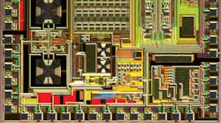
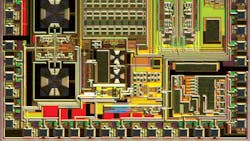
1. This highly integrated circuit demonstrates the silicon CMOS heritage of this SiGe device technology. (Photo courtesy of IBM.)
In contrast, an FET’s terminals are the gate, source, and drain—a voltage at the gate can control a current between source and drain. A FET is also known as a unipolar transistor because it uses only one form of conductor, electrons, or holes. Current flows from the drain to the source, with the conductivity varied by the electric field that is produced when a voltage is applied between the gate and source terminals. The current that flows between the drain and he source is controlled by the voltage between the gate and the source. FETs, in both silicon and GaAs forms, can be used as switches (as they often function in digital circuits or power supplies) or as amplifiers (providing gain to a circuit).
Silicon metal-oxide-semiconductor FETs (MOSFETs) are capable of high power-handling capabilities at lower (such as audio) frequencies and in switching power supplies. GaAs FETs—although not capable of the high power levels of silicon MOSFETs—can operate through microwave and millimeter-wave frequencies, typically in solid-state low-noise or power amplifiers. FETs can provide current gain, voltage gain, or both.
In addition to serving for many years as the substrate of choice for many high-power silicon bipolar transistors at sub-microwave frequencies, silicon has also been the basis for many high-frequency CMOS integrated-circuit (IC) devices. When fabricated with sufficiently small dimensions, such as with 90-nm processes, silicon CMOS transistors are capable of low-power, high-gain operation at frequencies to 60 GHz and beyond. While such devices have long been associated with digital and computer applications, their low cost and capabilities for millimeter-wave operation make them attractive candidates for use in higher-frequency consumer applications. These include point-to-point backhaul radios at 60 GHz and automotive radar systems at 77 GHz.
As part of efforts to develop higher-frequency, higher-power transistors, silicon has also worked with other elements as part of compound materials substrates, including silicon germanium (SiGe) and silicon carbide (SiC). SiGe substrates have held great promise for higher-frequency applications while silicon-carbide (SiC) materials offer much potential for higher power levels, whether as the main semiconductor substrate or as a base for other types of semiconductors.
IBM has done a great deal of work on high-frequency SiGe BiCMOS devices, offering foundry services for customers needing high-frequency analog and mixed-signal ICs. IBM’s SiGe technology is based on 130-nm silicon CMOS foundations, and is suitable for applications at 60 GHz and higher frequencies (Fig. 1). The firm offers what are known as “multi-project wafers,” with a number of different customers having their designs fabricated on the same wafer so that one customer is not required to field the expenses for an entire process run (for more, click here).
Last year, Renesas Electronics announced its work using a blend of SiGe and carbon, resulting in its model NESG7030M04 SiGe:C heterojunction bipolar transistor (HBT) for low-noise applications. Developed for 5-GHz wireless-local-area-network (WLAN) applications, this transistor features a noise figure of only 0.75 dB with about 14-dB gain in the 5.8-GHz band. This performance represents a significant improvement in noise-figure performance over the company’s earlier SiGe HBT devices. The firm explains that the addition of carbon has made it possible to optimize the device’s collector-base profile, increasing the range of supply voltages that can be used.
In terms of SiC, these discrete devices and modules are capable of high-voltage, high-power operation through lower microwave frequencies. An early developer of the technology, Cree, offers SiC MOSFET die and packaged devices at voltages to 1200 V, such as the low-frequency model CMF10120D. Suitable for motor drives and switched-mode power supplies, it draws 24 A at +1200 VDC.
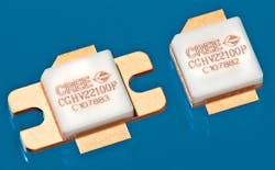
Over a decade ago, the firm introduced its model CRF-22010, a SiC MESFET capable of 10 W output power and 12-dB gain at 2.2 GHz. The Class A linear transistor is designed for a +48-VDC supply. But the company is also heavily involved in GaN device development, recently introducing 50-V GaN HEMTs for commercial cellular communications applications, including model CGHV22100 with 100 W output power from 1800 to 2200 MHz for Long-Term-Evolution (LTE) cellular base stations. The GaN HEMT (Fig. 2) features 20-dB gain with as much as 35% power-added efficiency across its frequency range.
2. These packaged 50-V GaN HEMTs are capable of 100 W output power from 1800 to 2200 MHz for use in cellular communications networks. (Photo courtesy of Cree.)
Many companies are finding the electrical capabilities of GaN and the thermal capabilities of SiC to be a powerful combination, fabricating GaN-on-SiC transistors with excellent high-power, high-frequency capabilities. The model T1G4005528-FS transistor from TriQuint Semiconductor is a discrete GaN-on-SiC HEMT that is usable from DC to 3.5 GHz. It provides 15-dB linear gain at 3.5 GHz with 55-W output power at that frequency when operating from a +28-VDC supply. It is built with the firm’s 0.25-μm production GaN process and supplied in a metal-ceramic flange package. It is suitable for commercial and military applications in radios, radar, and avionics systems. The company’s highest-power discrete GaN-on-SiC HEMT is model TGF2023-20, with 100 W output power from DC to 18 GHz. It offers maximum power-added efficiency of 52%, with 17.5-dB power gain at 3 GHz.
Just what kind of output-power levels are in store for GaN devices? Military organizations such as DARPA foresee GaN amplifiers as compact solid-state replacements for vacuum-tube electronics in radar systems. As an example, the Beverly Microwave Division of Communications and Power Industries developed their model VSS3607 GaN amplifier for S-band radar transmitters. It yields 1.3 W saturated output power from 2.7 to 2.9 GHz when operating with pulse widths from 1 to 100 μs at 10% duty cycle. The GaN amplifier draws 13 A at +30.5 VDC and provides 62-dB small-signal gain. It measures 9.5 x 15.5 x 1.75 in. and weighs 11 lbs. When 12 of these units are power combined as the model VSS3605 amplifier, however, they achieve 13 kW output power from 2.7 to 2.9 GHz with 71-dB small-signal gain. Of course, with so many amplifiers, the package size is somewhat larger, at 19.0 x 25.5 x 23.5 in. and 230 lbs.
Researchers pursuing higher-frequency uses for semiconductor devices have considered the various types of transistors and semiconductor devices used for microwave and millimeter-wave applications; they have generally compared GaAs versus GaN devices, or even InP devices. [Last year, NASA’s Jet Propulsion Laboratory (JPL) reported InP ICs operating to frequencies as high as 670 GHz.] For example, emerging applications in the terahertz (THz) region, which typically includes frequencies just below the infrared region, from 100 GHz to 10 THz, show a great deal of promise for imaging radar, and broadband communications systems.
The thermal conductivity of GaN is much higher than that of GaAs, about 170 W/m-K for GaN versus about 50 W/m-K for GaAs, which allows for much higher power levels for GaN devices compared to GaAs transistors. GaN also offers more than twice the bandgap energy of InP and GaAs. Quite simply, GaAs and InP transistors are limited in output power at higher frequencies, especially compared to GaN, making GaN an attractive semiconductor material for potential THz applications.
In addition, DARPA has invested in InP device technology for higher frequencies as part of its THz Electronics program. The organization’s efforts have resulted in improvements in InP HBTs and HEMTs, making possible a 670-GHz LNA based on InP active devices, as compact, lower-power replacements for vacuum-electronics devices. Major defense contractors, such as Northrop Grumman, have long applied InP HEMT MMIC technology for fabrication of amplifiers and other components operating in the millimeter-wave range, at frequencies past 200 GHz, for passive imaging and other satellite-communications (satcom) applications.


