InP IC Technology Powers Instruments Past 100 GHz
This file type includes high resolution graphics and schematics when applicable.
Next-generation high-speed digital interfaces are quickly and dramatically changing the requirements for millimeter-wave test-and-measurement (T&M) instruments. For the first time, millimeter-wave components and systems have the potential to reach the masses, in such applications as Fifth-Generation (5G) cellular communications systems, terabit-rate coherent optical modulation communications, and systems based on the upcoming IEEE P802.3bs 400G standard. All of these applications will require test equipment at millimeter-wave frequencies once considered more experimental than practical, but requirements for bandwidth as faster data rates are creating real needs for those higher frequencies.
Engineers working in these areas will need test equipment that supports operating frequencies above 60 GHz, data rates faster than 32 Gbaud, and the capability to transmit and receive multi-level coherent modulation formats in multiple-input/multiple-output (MIMO) signaling technologies. The performance of these test instruments is primarily set by the characteristics of the analog front end, which encompasses integrated circuits (ICs) that process analog signals between an instrument’s RF input connectors and its data converters.
Several years ago, Keysight Technologies took a fresh approach to instrument front-ends by applying indium phosphide (InP) semiconductor technology.1 ICs fabricated with Keysight’s first-generation InP process now power many instrument front-ends, including several of the company’s real-time oscilloscopes.2 Now, with the recent announcement of next-generation real-time and equivalent-time oscilloscopes,3 ICs fabricated in Keysight’s second-generation InP process are paving the way for high-performance instruments that reach beyond 100 GHz.
Exploring InP Technology
Hetero-junction bipolar transistors (HBTs) inherently achieve high RF power levels and high gain per unit area, excellent current gain and turn-on voltage uniformity, large transconductance, and low 1/f noise. The superior material properties of InP yield HBT devices with very high speeds, low resistances, high breakdown voltages, and semi-insulating substrates.
These beneficial properties enable the design of ICs for test-and-measurement instruments with low noise and high dynamic range beyond 100 GHz. For example, device and process engineers at Keysight’s High Frequency Technology Center have successfully scaled the existing InP process1 by shrinking lateral dimensions, applying advanced epitaxial design, and optimizing dielectric materials and metallization. The second-generation process achieves delay times on the order of 2 ps and maximum frequency of oscillation (fmax) approaching 600 GHz while maintaining breakdown voltages above 7 V for high output voltage swings and current gain greater than 50 for robust IC design.
Flexible layout options are available for designs that include any combination of high-speed, low-noise, and low-power attributes. This includes active and passive circuit elements (such as HBTs, diodes, thin-film resistors, and capacitors), enabling creation of digital, mixed-signal, and precision analog ICs for next-generation test instruments. The 3-in.-wafer, semiconductor fabrication process is well suited for low development costs and economical fabrication of very-high-mix ICs in low-to-moderate quantities.
HBT performance has been optimized for instrument-specific requirements. HBT epitaxial design is a key element in determining high device performance, and several major tradeoffs must be optimized to realize performance goals. Two-dimensional physical modeling was used extensively to understand process and circuit tradeoffs to develop the best devices for test-and-measurement instrument purposes.
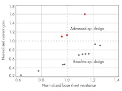
The three major components of the HBT—emitter, base, and collector—were all optimized. For the emitter and collector, doping and thicknesses were selected for the best balance of device speed, series resistances, and high-voltage operation. For the base, the key tradeoff is between base resistance (lower resistance enables higher speed) and current gain or beta. A minimum value of beta is required for robust circuit performance over the lifetime of the transistor. For Keysight instrument device technology, the base epitaxial structure was designed to accelerate electron flow through the base. This approach allows higher beta for a given base sheet resistance compared to more conventional base epitaxial designs (Fig. 1).
Excellent process control and reliability are essential for an instrument-grade technology that will be used to support a large number of IC and instrument designs. From the beginning of development, the design team emphasized yield, manufacturability, and reliability. To optimize process control, relatively large numbers of lots and wafers were processed, and extensive yield analysis was performed.
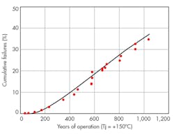
Processes were also optimized for achieving the best conditions of wear-out, infant mortality, and interconnect electro-migration reliability. The result has yielded devices with excellent instrument-grade reliability of less than 0.4% cumulative failures in 60 years of instrument life (Fig. 2). In addition, specialized devices provide built-in electrostatic-discharge (ESD) protection of more than 2 kV.
InP is a workhorse semiconductor process technology ideally suited for a wide range of IC types and topologies, ranging from simple passive multipliers and mixers to complex differential pulse amplifiers and multimodulus prescalers. InP diodes and transistors enable creation of ICs with extremely wide bandwidths, large signal swings, low noise, and low dissipated power—all of which are key attributes of time-domain and millimeter-wave-frequency test-and-measurement instruments.
Two general-purpose ICs can be used as examples to highlight the performance capabilities of this second-generation InP HBT semiconductor process: a single-ended feedback amplifier and a differential limiting amplifier. Both ICs have been designed in a full front-to-back design flow using the Keysight EEsof Advanced Design System (ADS) electronic design automation (EDA) software, with Keysight HBT transistor models validated to 110 GHz.
A feedback amplifier provides a simple but effective demonstration of the useful frequency range of a semiconductor process. It consists of one or more interconnected transistors comprising a single gain stage surrounded by two feedback resistors that set the amplifier gain and return loss. At high frequencies, capacitances inside the transistor reduce the transistor gain and ultimately define the amplifier bandwidth.
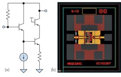
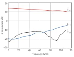
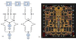
Figure 3 shows a schematic diagram and artwork for a recently fabricated feedback amplifier design. In this example, the gain stage is implemented in a cascode Darlington configuration that exhibits low input and output capacitances to maximize bandwidth. Figure 4 shows the measured small-signal S-parameters for this feedback amplifier. It delivers more than 10 dB gain and 10 dB return loss across a 90-GHz 3-dB bandwidth, making it a generic-but-versatile gain block for millimeter-wave instruments.
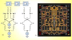
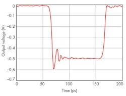
A differential limiting amplifier offers an alternate demonstration of the second-generation InP semiconductor process—one that is particularly useful for time-domain instruments that measure digital waveforms. In this amplifier, multiple cascaded gain stages amplify an input signal, saturating the output stage and producing a waveform with two well-defined voltage levels and very fast transitions between those levels. The example shown in Fig. 5 contains three gain stages implemented as Cherry-Hooper and cascode differential amplifiers. Figure 6 shows a measured 500-mV output waveform for a 5-GHz input signal. With less than 4 ps rise and fall times, this amplifier will find use in millimeter-wave instruments requiring ultralow jitter.
At millimeter-wave frequencies, a critical element of subsystem design is the monolithic-microwave-integrated-circuit (MMIC) package co-design. Maintaining MMIC performance to the front panel or subsystem connector requires thorough three-dimensional (3D) electromagnetic (EM) modeling. In addition, thermal modeling and validation helps ensure proper thermal management and reliable operation of components and circuits within a test instrument.
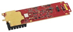
Finally, the large level of integration on a subsystem—such as millimeter-wave, RF, analog, and digital circuitry and their components—drives the need for a variety of packaging technologies to address each requirement at the optimal performance/cost point. Figure 7 shows an example of a complete front-end assembly that combines proprietary hybrid-on-printed-circuit-board (PCB) technology, with precision thin- and thick-film components and surface-mount-technology (SMT) components assembled in a compact 3 × 10-in. footprint.
Design validation and characterization are crucial and challenging to accomplish at millimeter-wave frequencies. The ability to extract and match more data to models often translates into faster convergence on the desired performance in the next MMIC design turn. For circuits of the complexity required for high-speed-digital and millimeter-wave test equipment, the required suite of tests ranges from classic frequency-domain S-parameter measurements to measurements of differential S-parameters/compression/harmonics combined with time-domain characterization.
The performance demands of next-generation high-speed digital interfaces are quickly and dramatically changing the requirements for millimeter-wave test-and-measurement instruments. Engineers working on technologies such as 400-Gb Ethernet, terabit optical, and 5G wireless communications will need test equipment that meets next-generation requirements for higher speeds, lower noise, lower power dissipation, and higher dynamic range. ICs fabricated in Keysight’s second-generation InP process are paving the way for high-performance instruments that reach beyond 100 GHz.
Robb Shimon, MMIC Design Manager, Integrated Circuit Design
Mathias Bonse, R&D Engineer, Compound Semiconductor Devices and Processes
Mario Righi, Package and Test Manager, Millimeter-Wave Module Design
Don D’Avanzo, Integration Engineering Manager, Compound Semiconductor Devices and Processes
Keysight Technologies, Inc., 1400 Fountaingrove Pkwy., Santa Rosa, CA 95403; (707) 577-2663
References
1. Tom Low, et al., “GaAs Sb DHBT IC Technology for RF and Microwave Instrumentation,” IEEE Compound Semiconductor Integrated Circuit Symposium, 2005.
2. Robert Shimon, et al., “InP IC Technology Powers Agilent’s Infiniium 90000 X-Series Real Time Oscilloscopes,” IEEE Compound Semiconductor Integrated Circuit Symposium, 2010.
3. Press release, Keysight Technologies, Inc.
Looking for parts? Go to SourceESB.
This file type includes high resolution graphics and schematics when applicable.
