LDMOS RFICs Gain Ground in Small Cells
This file type includes high resolution graphics and schematics when applicable.
Cellular wireless-communications-link handsets and their users throughout the world are often located by large base stations, and transmissions from those base stations are typically powered by discrete silicon LDMOS RF/microwave power transistors. But with increasing use of smaller cells to provide wireless coverage at the edges of large cells—in shopping centers, airports, and other public places—LDMOS RF integrated circuits (RFICs) are supplying the transmission power rather than discrete devices.
These rugged RFICs have benefited from advances made in discrete silicon LDMOS devices. Now they can provide the transmit power levels needed by small cells, while at the same time meet the tight space and power requirements of those compact wireless cells.
Commercial silicon LDMOS RFICs, such as the Airfast family of devices developed by NXP Semiconductors, are capable of output-power levels from 5 to 500 W per device at frequencies from 728 to 2,700 MHz. Advances in this technology have moved it beyond the limits of several years ago—such as top operating frequencies of 2 GHz—to achieve impressive power levels at frequencies to 2.7 GHz and devices with usable performance at frequencies as high as 3.8 GHz, or at frequencies beyond those used by any wireless carrier.
RFIC Advantages
One of the greatest benefits of an RFIC compared to a discrete transistor is the integration of the carrier and peaking stages of a Doherty amplifier within a single package. Matching circuitry is implemented on the RFIC semiconductor die rather than externally, such as on the printed circuit board (PCB) on which a discrete transistor is mounted, to reduce size and cost.
Of course, the package must be able to protect the RFIC as well as effectively dissipate excess heat from the device, and overmolded plastic packages have been significant contributors to the high levels of performance now possible with silicon LDMOS RFICs. While it might seem logical that a package made from ceramic should be more rugged and potentially have better performance than one made of plastic, just the opposite is true even at high RF power levels.
These plastic-package benefits are achieved in several ways with LDMOS RFICs, as well as discrete LDMOS transistors from NXP Semiconductors. First, the RFIC or transistor die is mounted on a copper heat spreader instead of a copper-based laminate. Since copper has high thermal conductivity of 350 to 400 W/m-K, it can reduce thermal resistance by 20% compared to a high-power RFIC or discrete device operating at the same output-power level and housed within a ceramic package with copper-topped laminate.
Lower thermal resistance allows more RF/microwave power to be handled than with an air-cavity package of the same size. This has been demonstrated at NXP by comparing one of the firm’s high-power Airfast LDMOS discrete devices housed in a plastic package to the same power transistor mounted in an air-cavity housing. For the same test frequency, the power transistor mounted in the plastic Airfast package produced 282 W output power at 1-dB gain compression, while the power transistor in the air-cavity housing produced only 260 W output power at 1-dB compression.
Designers of high-power PCBs are well aware of the importance of a laminate’s coefficient of thermal expansion (CTE) and how it compares to that of other materials, such as copper, that are used with the PCB dielectric material. This is a measure of how a material alters dimensionally with changes in temperature—notably, how much expansion takes place at elevated temperatures that, in a high-power transistor or RFIC, stem from the semiconductor device itself.
The copper heat spreader used in the Airfast device package reduces mismatches between the CTE at the solder joint between the package leads and the PCB, as well as between the heat spreader and the coin or pallet upon which it is soldered. Since gold metallization is not required with ceramic packages or with plastic Airfast packages, it eliminates problems caused by gold embrittlement of the solder joint.
In addition, the very tight dimensional tolerances achieved in plastic-packaged Airfast LDMOS RFICs results in excellent device-to-device repeatability. This provides, for example, consistent amplitude and phase performance for small cells using these silicon LDMOS RFICs for wireless signal amplification.
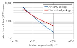
At one time, plastic packages were assumed to lack the long-term reliability of ceramic housings, but that is not the case with these advanced Airfast LDMOS RFIC packages. More than 3.5 million device test hours have been logged by NXP Semiconductors at various maximum junction temperatures for overmolded plastic packages, and 3 million test hours for air-cavity metal-ceramic packages.
Failure in time (FIT) and mean time to failure (MTTF) of both package types are nearly 1,900 years at a maximum junction temperature of +150°C (Fig. 1). Plastic packages maintain good longevity at higher junction temperatures.
Wireless applications for LDMOS RFICs require circuits capable of handling ever-wider bandwidths. As wireless communications networks evolve, they follow a trend of consuming wider bandwidths because of the growing number of users and the ways in which they use their wireless devices. Higher data rates are needed for the increased transmission of streaming video, which has become the greatest contributor to network traffic.
For example, the current generation of Long-Term-Evolution (LTE) cellular communications uses signal bandwidths as wide as 100 MHz. By 2020, or when Fifth-Generation (5G) wireless communications systems are deployed, the consumed bandwidth will have grown to 400 MHz or more. To put this in perspective, signal bandwidths in Second-Generation (2G) wireless networks were 5 MHz, reaching as wide as 40 MHz in the initial versions of LTE systems.
Addressing these challenges begins at the device level, where parasitic capacitance and its relationship to inductance affect a device’s signal bandwidth. The drain-source capacitance at the output of an LDMOS field-effect transistor (FET) combines with the inductance of the circuit board and the wire bonds used to attach the device to surrounding circuitry, resulting in resonances. Reducing the physical distance between interconnections, however, lowers the inductance (and resulting resonant effects) and increases the signal bandwidth of an RFIC’s active device.
In an Airfast LDMOS RFIC, this is accomplished by the addition of leads, bringing the FET electrically closer to the surrounding circuitry. This approach provides dramatic results, yielding signal bandwidths for a given device that are double those achieved with conventional device packaging. Development efforts show that bandwidth can be increased even further in the future to at least 200 MHz through this and other techniques, along with digital predistortion (DPD).
Achieving high isolation between in-package Doherty amplifiers is especially challenging, since its carrier and peaking (first- and second-stage) amplifier circuits are extremely close together in a miniature RFIC. The close proximity and high gain of these amplifier stages inevitably leads to crosstalk. Such crosstalk must be reduced to the lowest possible level, otherwise it will degrade performance of one or both amplifiers and linearization with DPD circuits will be more difficult.
Airfast Advances
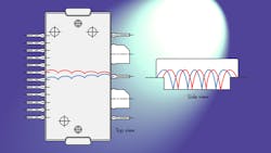
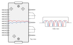
NXP developed a proven method for increasing isolation and reducing crosstalk, and implemented it for the first time in the company’s second-generation Airfast LDMOS RFICs. This technique, called a wire-bond fence, is an enhanced grounding structure that essentially stabilizes device package electrical connections. It is placed between the amplifiers and connected to grounding pins added to the input and output of the package (Fig. 2). The result is increased isolation between amplifier stages and an improvement in linearized adjacent-channel power (ACP) of 6 to 10 dBc.
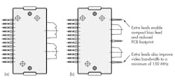
Enhancements to Airfast LDMOS RFICs are evident when comparing first-generation TO-270WB-14 and second-generation TO-270WB-17 packages (Fig. 3) from Freescale Semiconductor. In the latter, two pins were added to the lead frame, one originating at the device input and one from the device output, both of which terminate at ground on the board. This configuration, along with the wire-bond fence, together increase signal bandwidth and isolation between carrier and peaking amplifiers, as well as increase the frequency range of the RFIC. The output leads are spaced farther apart, too, which also increases isolation.
Furthermore, the new package saves board space by using dedicated dc bias leads instead of the large quarter-wave bias line present on first-generation Airfast devices. This saves between 30 mm 2 and as much as 90 mm 2 of circuit board space, depending on operating frequency. It also plays a role in broadening signal bandwidth.
On top of that, second-generation Airfast RFICs also make impedance matching easier and provide greater flexibility for optimizing performance at specific frequencies. For example, as the input of Airfast RFICs is internally matched to 50 ⦠and blocked with a capacitor, input impedance matching is not required. The devices’ output impedance has been increased to between 4 and 10 â¦, higher than the 1 to 2 ⦠typical of a discrete device and closer to the 50-⦠characteristic impedance of the surrounding circuitry.
Narrowing the impedance “gap” between the device and circuit simplifies design. Matching components embedded in the devices are optimized using electromagnetic simulation tools to improve quality (Q) factor and thus minimize losses, while also eliminating the inevitable variations that occur when using external matching components.
In some parts of the world, cellular networks operate over an extremely wide range of frequencies, from about 700 MHz to 3.8 GHz, requiring several amplifiers to achieve necessary signal transmission strength over such wide bandwidth. If possible, reducing the number of amplifiers can produce major cost savings while simplifying system design and reducing power consumption and size.
Currently available (second-generation) silicon LDMOS Airfast RFICs operate over multiple adjacent frequency bands, such as those from 703 to 960 MHz or 1,805 to 2,170 MHz. Meanwhile, a single LDMOS RFIC (model AFT27007N) can cover the range from 728 to 3,600 MHz.
LDMOS RFICs have significantly advanced in almost every respect within the last five years to address the demands of current cellular wireless communications systems, as well as to serve the expected needs of future systems. Current plastic-packaged devices can cover extremely broad frequency ranges while delivering considerably better performance than those in air-cavity ceramic packages. They can also accommodate very wide signal bandwidths and are achieving higher and higher levels of functional integration. There is little doubt that the performance of RFICs will keep pace with the continuing challenges posed by more complex networks.
Margaret Szymanowski, RF Design Engineering Manager
Suhail Agwani, Portfolio Manager, Small Cells
NXP Semiconductors, RF Power Business Unit, 1300 North Alma School Rd., Chandler, AZ 85224; (480) 814-4000
This file type includes high resolution graphics and schematics when applicable.


