Download this article as a .PDF
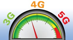
Expectations are high for Fifth-Generation (5G) cellular wireless networks, even though they are still several years in the making. Until then, 3G and 4G networks are and will be in service, requiring RF hardware that can provide reliable 3G and 4G performance while enabling a transition to the performance levels needed for 5G systems.
The latest member of the RadioVerse family of highly integrated transceivers from Analog Devices, the AD9375, provides the performance and flexibility to make the transition, stacked as it is with a fully integrated digital pre-distortion (DPD) solution, multiple receivers and transmitters, on-board frequency synthesizers, and a broad RF range from 300 MHz to 6 GHz for signals from a number of different wireless standards. In spite of the extensive functionality, it is a low-power-consumption device (5 W) well suited for use in small wireless base transceiver stations (BTS) where power and size must be conserved, such as those employing large numbers of antennas in massive multiple-input, multiple-output (MIMO) configurations.
Radio designers are facing some severe challenges for 4G wireless networks, let alone for eventually emerging 5G networks. As the numbers of wireless users, both people and things, continue to grow at such a rapid pace worldwide, BTSs and small cells must provide high performance with the flexibility to meet dynamic operating conditions and requirements. Users will be people expecting everything they can get from a smart cellphone, and probably an even greater number of things, in the form of Internet of Things (IoT) sensors and other IoT devices.
Seamless wireless coverage and service for this growing number of users will be made possible by more BTSs and an increasing number of small cells; in particular, the small cells help to prevent gaps in the wireless coverage such as in large office buildings. The AD9375 is an excellent starting point for these small cells because of its low power consumption, multiple receivers and transmitters, and flexible software-defined-radio (SDR) architecture. Since 5G standards are being formulated in terms of center frequencies, bandwidths, and modulation schemes, the AD9375 provides the coverage and programmability to tune where it is needed when those standards come, while still meeting current 4G requirements.
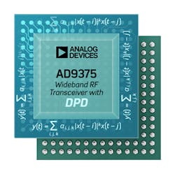
The AD9375 (Fig. 1) includes an impressive number of transmit and receive functions in a single 12 × 12 mm BGA packaged device with a tunable frequency range of 300 MHz to 6 GHz. Fabricated with a 65-nm silicon CMOS semiconductor process, it contains dual differential transmitters, dual differential receivers, an observation receiver with two inputs, a sniffer receiver with three inputs and, most importantly, the on-chip capability to linearize a connected high-power transmit amplifier with a digital-predistortion (DPD) algorithm. The AD9375 integrates a low-power DPD actuator and adaption engine for improving the linearity of a connected transmit power amplifier (PA), so that transmit linearity can be achieved without the power consumption normally associated with such functionality.
The AD9375 transceiver is similar to its predecessor, the AD9371, with two 100-MHz receivers, two 250-MHz transmitters, a two-input observation receiver, and a three-input sniffer receiver, with system-level interconnections via a 6-Gb/s JESD204B interface. In fact, the packaged devices are pin-for-pin compatible. The integrated DPD circuitry within the AD9375 provides transmit linearity without excessive power consumption, especially enticing for small cells. It features instantaneous bandwidth as wide as 40 MHz for 3G and 4G waveforms. Compared to off-chip DPD methods based on field-programmable gate arrays (FPGAs), the on-chip circuitry can effectively linearize a transmit PA with as much as a 90% reduction in power consumption. Performing the DPD functionality with on-chip circuitry also simplifies the system-level design of a BTS or small cell, cutting the number of JESD204B interface lanes in half and requiring less FPGA resources.
The AD9375 features fully integrated and independent fractional-N frequency synthesizers to generate the local oscillators (LOs) required for transmit, receive, observation receiver, and clock functions. The transmitters and receivers support frequency-division-duplex (FDD) and time-division-duplex (TDD) operation.
The AD9375’s differential transmitters produce large-signal bandwidths as wide as 250 MHz from 300 MHz to 6 GHz. When used for a 3G system such as the Universal Mobile Telecommunications System (UMTS), the LOs offer signals at 700, 2600, 3500, and 5500 MHz with as much as +7 dBm output power at 700 and 2600 MHz, as much as +6 dBm output power at 3500 MHz, and as much as +4 dBm output power at 5500 MHz.
Across those wide transmit bandwidths, the typical amplitude flatness is ±0.5 dB, with typical deviation from linear phase within 10 deg. The transmit power can be controlled over a range of 0 to 42 dB with power control resolution of typically 0.05 dB. In spite of the small size of the AD9375, the different transmitters are well isolated, from each other and from the receivers. The transmitter-to-transmitter isolation ranges from 65 dB or better for the 700-, 2600-, and 3500-MHz LOs to 50 dB for the 5500-MHz LO. The isolation between the two main receivers and between either of the receivers and any of the transmitters is typically 60 dB or better.
Receiving the Future
The AD9375’s receivers are also tunable from 300 MHz to 6 GHz, offering a gain range of 0 to 30 dB in 0.5-dB gain steps. The gain amplitude flatness is within ±0.5 dB. The receive bandwidth can be set from 8 to 100 MHz. The maximum recommended input signal power to the receivers is -14 dBm at 0-dB attenuation. The receiver noise figure ranges from 12 dB with the 700-MHz LO to 18 dB with the 5500-MHz LO, while its input third-order intercept point (IIP3) performance is remarkably consistent with frequency, varying only from typically +22 dBm for operation with the 700-MHz LO to typically +20 dBm for operation with the 5500-MHz LO.
In addition, the AD9375 includes a two-input observation receiver and a three-input sniffer receiver. The observation receiver has a tunable center frequency range from 300 MHz to 6 GHz with gain range of 0 to 18 dB; maximum input levels shouldn’t exceed -13 dBm. The typical amplitude ripple is ±0.5 dB across a 250-MHz bandwidth. For the same receiver bandwidth, the deviation from linear phase is typically ±10 deg. The sniffer receiver has two input ports with low-noise amplifiers (LNAs) for detecting signals across 20-MHz bandwidths from 300 to 4000 MHz.
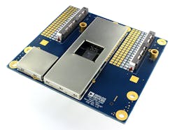
The AD9375 transceiver is supplied in a 196-ball BGA--a small package with large benefits. However, it is not left to wireless system designers to extract those benefits. The AD9375 is supported by a large number of models and commercial modeling tools, including MATLAB and Simulink from MathWorks, to help speed the prototypying process. In addition, the transceiver is available as part of an evaluation kit and as a reference design. The reference design, developed in partnership with radio systems designer Benetel Ltd., supports LTE with 20-MHz channels in a two-transmitter, two-receive system configuration with 250-mW output power per antenna. The reference design (Fig. 2) is a circuit measuring just 88 × 83 mm that consumes less than 10 W power.
Analog Devices Inc., 804 Woburn St., Wilmington, Mass 01887; (781) 329-4700


