Download this article in PDF format.
Gallium-nitride (GaN) technology’s impact on the RF/microwave industry cannot be overstated, as it’s enabling applications from space and military radar to cellular communications. And while GaN is generally associated with power amplifiers (PAs), it has other use cases as well. GaN’s journey since its introduction has been fascinating, and it’s likely to be even more so as we enter the era of 5G.
GaN’s Role in the Radar and Space Realms
Two variants of GaN technology are GaN-on-silicon (GaN-on-Si) and GaN-on-silicon-carbide (GaN-on-SiC). GaN-on-SiC contributes heavily to space and military radar applications, according to Damian McCann, director of engineering, RF/microwave discrete products group at Microsemi. “Today, RF engineers are finding new applications and solutions to take advantage of the ever-enhanced power and efficiency performance levels achieved by GaN-on-SiC devices, notably in space and military radar applications.
“With GaN being a wide-bandgap semiconductor material that provides high levels of hardness, mechanical stability, heat capacity, very low sensitivity to ionizing radiation, and thermal conductivity, clever designs result in even greater size, weight, and power (SWaP) advantages. We have also seen GaN-on-SiC technology outstrip once competitive technologies—even at lower frequencies.”
System designers stand to benefit from GaN-on-SiC technology. McCann explains, “Thermally enabled and highly integrated laminate technology, when coupled with GaN-on-SiC, is allowing the system designer to now look to even greater levels of integration, notably extending primary radars to cover multiple bands in the same physical area and adding increased secondary radar functionality. Applications within the space market have also recently seen an increase in GaN-on-SiC feasibility work, notably in applications in which the efficiency of GaN is complemented by the ability to operate at ever-higher frequencies.”
He adds, “The power density of millimeter-wave (mmWave) GaN brings a new set of design techniques looking for even greater levels of back-off. Solutions must extend beyond power and linearity in power back-off, but also to when power control is needed or when operating into variable levels of VSWR.”
McCann also notes that GaN-on-SiC technology makes it possible to replace older klystron technology. He says, “The general application of active electronically scanned arrays (AESAs) and phased-array elements in military and commercial space applications is also looking to take further advantage of GaN-on-SiC monolithic-microwave-integrated-circuit (MMIC) integration to reach new levels of power—even replacing aging klystron technology in some cases.
“The most notable absence from the market, though, is the number of qualified 0.15-µm GaN-on-SiC foundries. This is something the whole industry is only too readily aware of as roadmap developments take shape addressing these exciting new applications.”
GaN and 5G Communications
GaN technology isn’t limited to space and radar applications, though. It’s driving innovation in the arena of cellular communications. And what about the 5G networks of the future? What role will GaN have there?
Somit Joshi is senior director of metal-organic chemical vapor deposition (MOCVD) product marketing at Veeco Instruments. He says, “The ambitious scope of 5G promises to transform cellular communications, creating new opportunities for carriers and service providers. 5G is currently being planned with a vision of greater than 10 Gbps transmission speeds for mobile broadband (phones/tablets/laptops) and ultra-fast low latency for Internet of Things (IoT) applications.”
Joshi adds, “Today, GaN is slowly replacing silicon (Si) in specific applications (i.e., RF amplifier front ends of 4G/LTE base stations). Next-generation 5G deployment will involve additional use of GaN technology. Pre-5G, there was increasing use of GaN-on-SiC in the macro cell. 5G will bring in GaN-on-Si to rival GaN-on-SiC designs with inroads into the small cell space (micro/metro cells) before potentially overlapping into femtocells/home routers and even into handsets.”
GaN technology will be critical in terms of the higher frequencies expected to be used by 5G networks, according to Joshi. He explains, “5G will deploy gradually over time and in multiple frequencies. Two primary frequency ranges will be sub-6-GHz for wide-area coverage and frequencies greater than 20 GHz (mmWave bands) for high-density areas like stadiums, airports, etc. For 5G technology to meet stringent expectations (faster data rates, low latency, massive broadband), new GaN innovations will be needed to enable higher targeted frequencies (i.e., 28- and 39-GHz bands).”
Furthermore, GaN technology will be well suited for 5G handsets. Joshi adds, “From a technology standpoint, 5G suffers from attenuation issues, requiring multiple antennas to improve signal quality using spatial multiplexing techniques. Each antenna requires dedicated RF front-end chipsets. Compared to gallium arsenide (GaAs) and Si, GaN has less antenna requirements for the same power levels. The resultant form factor advantages make GaN ideally suited for 5G handsets.
“Moreover, higher power efficiency and lower transmission losses result in significant power savings. Integrating multiple GaN transistors monolithically opens up new functionality and capability. GaN has some limitations when operating at lower voltages (less than 5 V)—issues being worked on by process experts, integrated device manufacturers (IDMs), and research institutes.”
1. The film-deposition control provided by Veeco’s Propel GaN MOCVD system helps improve buffer quality.
Lastly, Joshi explains what Veeco brings to the table. “We are at the forefront of GaN-on-Si development in collaboration with leading device companies and research institutes. Leveraging the single-wafer TurboDisc technology that provides dopant control and compositional uniformity while reducing the cost-per-wafer, we are helping customers solve tough challenges of RF loss, transistor performance, harmonic distortion, and device reliability. This is achieved by leveraging the Propel MOCVD system’s superior film-deposition control for buffer quality improvement and its capability to incorporate hard-to-deposit materials like InAlN, etc. (Fig. 1).
“The market for GaN-on-Si and GaN-on-SiC is small and challenges persist as tools and processes still need to mature to increase yield and throughput,” continues Joshi. “However, we see significant potential as use cases continue to proliferate with process and technology improvements for 5G applications.”
Beyond Power Amplifiers: GaN-Based Low-Noise Amplifiers
In the RF/microwave industry, GaN technology is typically associated with power amplifiers. But one company, Custom MMIC, is demonstrating that GaN does indeed have other use cases by developing low-noise amplifiers (LNAs) based on GaN technology.
“We are often asked why we developed a line of GaN high-electron-mobility-transistor (HEMT) LNAs at microwave frequencies when GaAs pseudomorphic-high-electron-mobility-transistor (pHEMT) LNAs are much more common,” says Chris Gregoire, senior applications engineer at Custom MMIC. “The reason is simple: GaN offers more than just low noise.
“For one, GaN has much higher input power survivability, which can greatly reduce or eliminate the front-end limiter often associated with GaAs pHEMT LNAs. By eliminating the limiter, GaN can also reclaim the loss of such a circuit, thereby lowering the noise figure even further. Second, GaN LNAs have much higher output third-order intercept point (IP3) than their GaAs pHEMT counterparts, which improves receiver linearity and allows for greater sensitivity.”
Gregoire continues, “One main reason GaN offers such advantages is its inherently high breakdown voltage as compared to GaAs processes. When an LNA is overdriven, the gate-drain breakdown can induce failure. GaAs pHEMT devices have typical breakdown voltages of 5 to 15 V, which severely limits the maximum RF input power these LNAs can withstand. GaN processes, on the other hand, feature voltage breakdowns in the 50- to 100-V range, thereby allowing for much higher input power levels without damage. Additionally, the higher breakdown voltage allows GaN devices to be biased at higher operating voltages, which directly translates into higher linearity.
“We have learned to maximize the advantages of GaN and create state-of-the-art LNAs that have the lowest possible noise figure along with high linearity and high survivability. As a result, GaN is the preferred LNA technology for any high-performance receiver system, especially when immunity to jamming signals is a vital requirement.”
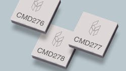
2. These three low-noise amplifiers were developed using GaN technology.
Custom MMIC recently announced three new GaN-based LNAs (Fig. 2). “We invite you to examine our three newest GaN LNAs,” says Gregoire. “The CMD276C4, which operates from 2.6 to 4 GHz, features 14.5 dB of gain, a noise figure (NF) of 1.2 dB, and an output IP3 of +32 dBm. The CMD277C4, which operates from 5 to 7 GHz, features 20 dB of gain, a NF of 1.2 dB, and an output IP3 of +33.5 dBm. The CMD278C4, which operates from 8 to 12 GHz, features 15 dB of gain, a NF of 1.8 dB, and an output IP3 of +33 dBm. Additionally, all three components can withstand a maximum continuous input signal of up to 5 W—with or without bias voltage applied.”
Simply put, GaN technology has become a major force in the RF/microwave industry. In the future, its role is likely to expand further due to 5G communications and more. And while GaN and PAs go hand in hand, one shouldn’t overlook the fact that LNAs are also being developed with the technology. To sum it all up, it might be time to catch onto GaN if you haven’t already, because its future looks bright.


