Shielded Anode PIN Diode Breathes New Life into a 1950s Technology
Download this article in PDF format.
The RF PIN diode as we know it today was invented by J. Nishizawa in 1950. Now, almost 70 years later, a new PIN diode concept—shielded-anode PIN diode (SAPIN)—has emerged. This new PIN diode offers 10 to 50 times better “OFF” isolation thanks to the introduction of a simple electrostatic shield. An “OFF” isolation greater than 40 dB at 2 GHz and 0 Vdc is achieved from a single series device. The theory of operation will be presented here along with measurements on fabricated silicon (Si) SAPIN didoes.
PIN Diode Operation
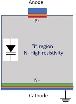
A PIN diode is built with a wide undoped intrinsic (i-region) semiconductor, usually Si or gallium arsenide (GaAs). The i-region is sandwiched between the p+ anode and the n+ cathode. Both are connected to a conducting metal like gold or aluminum (Fig. 1).
1. The anode and cathode are both connected to a conducting metal.
In contrast to conventional diodes, the wide i-region enables the PIN diode to operate as a fast RF switch or a current-controlled linear resistor. When forward-biased, the PIN diode operates under a high-level injection condition. At low frequencies, the PIN diodes behave as a normal diode and follow the same basic equations for current (I) versus voltage (V).
At low frequencies well below the carrier lifetime τ, the charge can be swept out and the diode turns “OFF.” At high frequencies, there’s not enough time to sweep the carriers out of the i-region and the diodes remain turned “ON.” The ac series resistance, Rs, is given by:
where:
τ = carrier lifetime in i-region (about 1 µs for Si, 10 ns for GaAs)
Q = Ifτ
W = i-region width (about 5 µm for switches, 200 µm for CATV attenuators)
If = forward-bias current
µn = electron mobility
µp = hole mobility
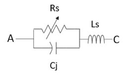
Figure 2 shows a simplified RF equivalent circuit for an RF PIN diode. The series resistance, RS, was already given. PIN diodes for RF switching typically have an RS of 10 Ω at 1-mA forward quiescent current. For linear attenuator applications, RS is typically 75 Ω. The parasitic series inductance, Ls, represents the bond-wire and package-lead inductance. The value for Ls is usually around 1 nH.
2. This is a simplified RF equivalent circuit for a PIN diode.
The capacitor Cj from the anode to cathode is due to the junction and fringing capacitance within the PIN diode. This capacitance is an unwanted parasitic. In RF switches and attenuator circuits, good isolation is important yet difficult to attain. Ultimately, the best isolation is limited by the magnitude of Cj.
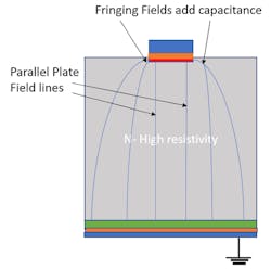
Under zero bias, the depletion region in a PIN diode will usually extend the whole distance across the i-region to the cathode due to the i-region’s undoped nature. Under zero bias, the electrostatic field lines will extend from the anode to the cathode (Fig. 3).
3. Field lines and fringing fields are shown in this illustration.
Figure 3 shows the field lines that would be considered as per the parallel-plate capacitance formula, as well as fringing field lines to the grounded cathode below. The total capacitance from the extra fringing fields can be much larger than that of the parallel-plate capacitance alone.
The SAPIN Diode
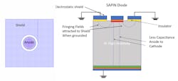
Figure 4 shows the top view of the SAPIN and a simplified cross-section drawing of the SAPIN diode.1 As a normal PIN diode, the device has a p+ anode, undoped i-region, and an n+ cathode connection. (Normally the cathode is the back-side of the device for a good ground connection, but the anode and cathode can be interchangeable.)
4. Shown are a top view of the SAPIN (left), as well as a simplified cross-section drawing (right).
A new shield terminal made of metal over an insulator is added around the anode, which in this case is SiO2. This shield has little effect on the dc RS characteristics of the PIN diode action. With 0 Vdc applied to the anode, part of the electrostatic field lines is drawn away from the cathode; instead, it’s terminated on the new shield terminal.
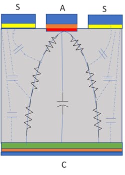
3D device simulations demonstrate that the value of Cj can be reduced by more than two to three times the total value, thereby dramatically improving the device isolation. The actual operation of the SAPIN is much more complicated than what the simplified electrostatic drawing indicates. Figure 5 shows a SAPIN turned “ON” that’s operating at low currents (approximately 10 µA to 1 mA). A simple distributed RC network has shown to be a rough model description of the SAPIN’s operation. The actual operation is very difficult to model due to the distributed nature of the parasitics, as well as a variable carrier lifetime.
5. Parasitic coupling exists between the shield and the anode as well as between the shield and the cathode.
As can be determined directly from Figure 5, parasitic coupling will occur between the shield (S) and the anode and between the shield and the cathode. Direct measurements will best allow for understanding and modeling of the actual device.
SAPIN Diode Measurements
Figure 6 shows a fabricated SAPIN. The device was made using 4-in. Si wafers with resistivity greater than 3000 Ω-cm. The die size is 350 × 350 µm with the i-region thickness varied from 250 to 375 µm. These devices are geared toward RF attenuator applications.
6. Shown is a fabricated SAPIN.
The anode, cathode, and shield metallization are aluminum. The measured effective carrier lifetime on Si wafer and die samples was determined to be about 1.5 µs.
One-port (S11) RF measurements were performed on the SAPIN diode between the anode, shield, and grounded cathode. The biggest concern involved the capacitive loading of the shield to anode and cathode, since the shield was also grounded. Devices were epoxied to a metal carrier, and a ground-signal (G-S) probe from GGB Industries was used to measure S11 from 50 MHz to 2 GHz.
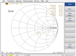
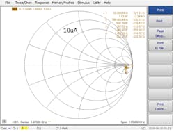
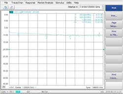
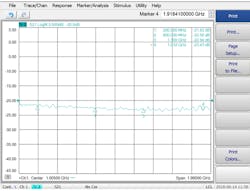
Figures 7 and 8 show S11 at a diode current of 2 mA, and a measured S11 at a forward bias of 10 µA, respectively. As can be seen, there’s a dramatic difference between the equivalent input capacitances at the two operation currents. At 2 mA, C = 34 pF and 4.1 pF at 50 MHz and 2 GHz, respectively. At 10 µA, C = 1.4 pF at 50 MHz and 0.35 pF at 2 GHz. The frequency dependence of capacitance is affected by the carrier lifetime and the distributed nature of the SAPIN (Fig. 5, again).
7. Shown is S11 with a diode current of 2 mA and shield grounded.
8. This is S11 with a forward bias of 10 µA and shield grounded.
Directly grounding the shield would be a disaster at higher currents, and the SAPIN would not be a usable device. Notice that at low currents, there’s a large resistive component to the input impedance. At high currents, RS is a very small value. One aspect discussed in Ref. 1 solves the loading problem. Figure 9 shows the solution.
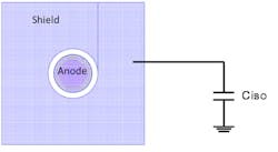
9. Here, an external capacitor is connected from the shield to ground.
A small external capacitor of about 0.3 pF, dubbed Ciso, can be directly connected to the shield to ground. At high currents, Ciso would look like a shunt capacitor to ground, and compared to 50 Ω, would be a relatively high impedance that doesn’t significantly affect the circuit. At low current, Ciso is in series with a small capacitance. This large series-resistance component would therefore not be detrimental to the circuit’s performance. At low currents, however, Ciso will produce effective reduction in fringing capacitance (Fig. 4, right).
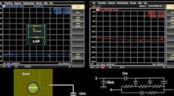
For two-port measurements looking into the anode and cathode terminals, the SAPIN was assembled in a SOT3 package with an external Ciso of 0.3 pF. Figure 10 shows the S21 measurement with 1 mA of dc bias current. The calculated series resistance is about 175 Ω.
10. With the SAPIN assembled in a SOT3 package and with an external capacitance of 0.3 pF, S21 was measured with 1 mA of dc bias current and a calculated series resistance of about 175 Ω.
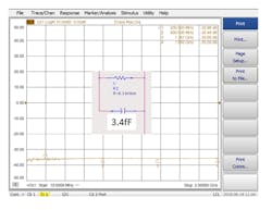
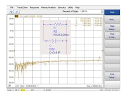
In Figure 11, RS is set to 1.25 kΩ. An RS-value of 6.3 kΩ for a variable feedback resistor is needed for a transimpedance amplifier application.2 Figure 12 shows the measured S21 at 6.3 kΩ, along with the Advanced Design System (ADS) lumped elements for the best-fit simulation. The equivalent capacitor across the 6.3-kΩ resistor is 3.4 fF, indicating an RC 3-db frequency of 7.2 GHz.
11. RS was set to 25 kΩ for this measurement.
12. This is the measured S21 with RS equal to 6.3 kΩ.
With 0 Vdc, the device current was set to 0 mA. Figure 13 illustrates the resulting “OFF” isolation exhibited by the SAPIN diode with best-fit resistor and capacitor values of 25 kΩ and 3.4 fF.
13. Shown is the SAPIN’s “OFF” isolation.
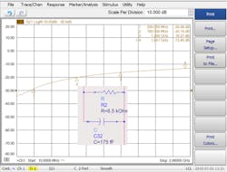
For comparison, an industry-standard SMP1307 attenuator PIN diode was measured at 6.3 kΩ. Figure 14 shows the two-port S21 response that results in a best-fit RC model of 6.5 kΩ and 175 fF. The 3-db bandwidth when using this device as a resistor would only be about 144 MHz. In Figure 15, S21 is in the “OFF” isolation case with 0 Vdc and I = 0 mA. The equivalent RC lumped-element fit is 175 fF/25 kΩ.
14. This is the S21 of an SMP1307 attenuator PIN diode with RS equal to 6.5 kΩ.
15. The SMP1307’s “OFF” isolation is revealed.
Conclusions
Device simulations show a dramatic improvement in device performance with the addition of the shield—but not as much as a 50× improvement. We suspect there’s additional attenuation due to the distributed nature of the SAPIN device as shown in Figure 5.
A lumped-element distributed circuit may help to explain the SAPIN broadband behavior (Fig. 16). It can be thought of in a similar manner as the old oscilloscope probe-compensation networks. There’s a voltage division with the resistances and capacitances together with the 50-Ω source and load impedances.
16. This circuit representation may provide insight into the SAPIN’s broadband performance.
Work needs to be done to further understand the exact details of the device operation. In addition, future work will look to integrate the compensation capacitor Ciso into the Cox capacitor between the shield electrode and silicon surface. As it stands now for oxide thickness tox of about 800 A, the value of Cox is in the range of 100 pF. Simplifying the capacitors will allow the shield to be directly grounded.
Robert Bayruns is Chief Technology Officer at Duet Microelectronics and Ashok Ramu is TCAD Developer at Silvaco.
References
1. Ramu, R Bayruns, and M Francois, “An Improved Isolation PIN diode,” US Patents Pending.
2. R Bayruns and T Laverick, “Automatic gain-control transimpedance amplifier,” US Patent 5646573 and US 5602510.
