Beyond CMOS Vs. GaAs: Picking The Right Technology
This file type includes high resolution graphics and schematics when applicable.
Matching a technology to a new product design is not always easy, since each technology offers its own benefits under different conditions. For example, the debate between silicon-CMOS and gallium-arsenide (GaAs) semiconductor technologies was lively at the recent 2013 IEEE International Microwave Symposium (IMS) in Seattle, WA. Comparing the two technologies is not as simple as comparing the performance levels of their active devices.
The best way to compare device technologies is by analyzing them as part of a technology mix in a completed product. To choose between a CMOS or GaAs power amplifier (PA) module, for example, the surrounding required technologies—including passive devices, laminate, packaging, and surface-mount device (SMD) components required for each PA—should also be evaluated. Design software can speed and simplify such comparisons, under different conditions.
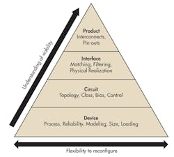
Product-level technology decisions are difficult because design tradeoffs must be considered as complexity is added to a base device technology. An informed comparison is possible by starting simply and rapidly adding complexity while evaluating corresponding technology tradeoffs. A methodical approach should be followed, where a proposed mix of technologies is evaluated by rapid virtual prototyping, starting at the device level and working through to the product level.
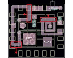
This way, the interactions between technologies can be evaluated within a proposed product. The results between two or more different technology combinations can then be compared at the top product level. This design methodology can be shown for GaAs- and CMOS-based technology mixes applied to PA module designs (Fig. 1).
With their high breakdown voltages and capabilities to handle high current densities, GaAs heterojunction bipolar transistors (HBT) are excellent active devices for RF/microwave PAs. To evaluate this design approach, the GaAs PA was based on the HBT process from WIN Semiconductors, which uses the Agilent HBT model from Agilent Technologies. Besides fitting the device characteristics well, this model has robust convergence, which is critical for large-signal co-optimization across different technologies. At the device level, the key design consideration is to mitigate reliability concerns. For a GaAs HBT PA, this means breaking the device into parallel fingers that are individually ballasted to prevent localized thermal runaway.
The design of a GaAs HBT PA will be based on a Class-E switch-mode configuration. One of the keys to this design is determining the required number of parallel active devices to achieve the target output power while also maintaining a long device operating lifetime. Since the circuit topology will drive the power and efficiency of this PA design, these needs should be evaluated at the circuit level. From the power requirements, it is possible to estimate the peak-to-peak and DC current levels to determine the number of device fingers. An electrothermal analysis can then be applied to verify the junction temperature.
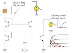
The bias and power-control requirements for this GaAs HBT PA design should also be considered at the circuit level. In this case, the power-control function is contained in a separate integrated circuit (IC) based on a standard silicon CMOS process and simulated using equation-based symbolic devices. A common technique for controlling the output power of an active device is biasing the device under voltage-saturated conditions and controlling the supply voltage with a regulator; unfortunately, this approach suffers loss.
For this type of technology evaluation, it is important to pay attention at the losses at each step of the design. Degradations in performance can change a decision concerning a technology—one reason why the “rapidly added complexity” design methodology can help guide the choice of technology mix (Fig. 2).
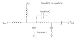
Textbook Class-E matching networks incorporate a resonator that enhances the harmonic short circuit provided by the switching capacitor. A more practical realization is a standard inductive-capacitive (LC) impedance match that uses SMD capacitors and laminate inductors to transform 50 Ω at the antenna to the lower device-level impedance of about 2 Ω. This works well when the shunt Class-E capacitor is physically close to the low-impedance active device (Fig. 3).
This file type includes high resolution graphics and schematics when applicable.
Design Considerations
This file type includes high resolution graphics and schematics when applicable.
For the physical design of the GaAs PA’s matching networks, an inductor layout will be created on a four-layer laminate with a FR-4 dielectric core that can be used to generate an electromagnetic (EM) model for optimization. Using the model can help select the proper inductor values and circuit dimensions for this PA application (Fig. 4). The EM modeling process is repeated for each inductor, and then a fully integrated match is optimized. Complexity is added to this design by replacing the ideal capacitors of the model with discrete-valued capacitors from Murata Manufacturing Co. Ltd. A realizable circuit design results by performing the optimization with these discrete components.
Then, the plan for developing the GaAs PA involves simulating the output impedance match with the PA. The simulation analysis reveals that the device-level efficiency is not affected by the output match; however, some loss is apparent from the nonideal output match, causing a slight decrease in the power-added efficiency (PAE) and output power (Pout) of the PA, as was expected. Although expected, it is important to monitor such losses at every step in the design process.
The next step in the GaAs PA design involves integrating the laminate with the GaAs PA and mounting it into a 3.5 x 3.5 mm package. For a quick evaluation, the top metal layer of the GaAs die was modeled with the laminate substrate, using a three-dimensional (3D) electromagnetic (EM) simulation of the bond wires to analyze their inductances and mutual coupling. This provides a good estimate of potential performance degradations at the interface level, essential when evaluating a technology mix.
To add even more realistic complexity to this analysis, the PA’s backside ground via holes were connected to the laminate’s ground paddle. When this was first done, the amplifier’s PAE dropped by 9% and the output power dropped by approximately 1 dB. Fixing such losses can be quite difficult at the product level. But at the interface level, it is possible to extract the small-signal ground inductance of the combined via and die-paddle structure.
Next, to troubleshoot the problem, an ideal via is replaced with a lumped inductor at the circuit level. It is easy at this point to change the load and source impedances to find a more optimal combination. Finally, at the product level, the output impedance match is adjusted to regain optimum PAE and output power. This demonstrates the power of this design approach, with the flexibility to tune and optimize the amplifier circuitry while also modeling the interconnections.
The GaAs-based design approach includes accurate model values for SMD capacitors, the circuit laminate, and the interconnections. To evaluate the viability of this technology mix and understand its tradeoffs, simulations are performed at the system level, with modulated sources to accurately model the signals in actual systems. Using the laminate with SMD components provides numerous advantages, including being simple, flexible, and providing an output match that is tunable and with high quality factor (Q). The disadvantages include the limited opportunities for size reduction with SMD components, a bias topology that degrades the amplifier’s PAE, and only limited use of the lower laminate layers.
For the PA using a CMOS-based technology mix, the power-control function will be integrated on the IC. The matching transformer could be integrated on the same IC but, for this design example, an integrated passive device (IPD) transformer will be used to better illustrate how to evaluate a less-conventional technology approach.
Active RF/microwave devices for PAs are typically large and must handle relatively high voltages, which is a challenge for devices with smaller CMOS gate lengths. Since transistor operation is based on a MOS capacitor in the CMOS-based mix, the dominant reliability mechanisms are related to breakdown voltages. The RF swing across the junctions is limited to 2x the device operating voltage, presenting a challenge to achieve RF output power above 1 W. Several approaches must be taken to mitigate this reliability challenge, approaches which span from the circuit to the interface levels, with tradeoffs existing among output power, circuit size, and reliability.
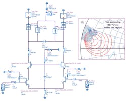
At the circuit level, a Class-E configuration works well because switching-mode operation mitigates reliability concerns across the gate-drain junction while a differential cascode topology divides the RF voltage-swing between several devices. Power control is performed in a closed-loop fashion by sensing the RF signal at the output and adjusting the bias voltage on the top cascode device.
This file type includes high resolution graphics and schematics when applicable.
Further Analysis & Conclusions
This file type includes high resolution graphics and schematics when applicable.
An initial load-pull analysis of a standard differential cascode topology reveals that the RF voltage swing is not well balanced between the upper and lower devices, with the upper device encountering a higher voltage swing. Using 2Vd as the reliability limit, a circular area on a Smith chart will show the region of unreliable operation which is, unfortunately, the entire usable range of the PA (Fig. 5). This is due to the load impedance presented to the bottom device, which is close to a short circuit since the cascode’s gate node is a virtual ground.
A more practical topology for the CMOS technology approach is one that allows for independent control of the cascode gate impedance. To achieve this, the gate feeds for the cascode device are broken up and separately terminated with a shunt capacitor. Once this is done, the voltages can be more evenly balanced across the devices, and the unreliable range of operation shifts outside the usable range of the PA.
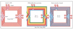
A good approach for improving reliability at the interface level is to use a transformer to combine, in parallel, several stacks of devices into a single load. This allows each stack to see less of a voltage swing. For the CMOS technology mix, a discrete transformer designed on a 10-μm-thick metal IPD process from ON Semiconductor was considered as a candidate.
Each primary turn is a different color that weaves from outer to inner turn, driven differentially. The secondary turn is one long series inductive coil to ground (Fig. 6). As with the GaAs technology mix, the transformer for the CMOS-mix PA was parameterized to create an optimizable EM model. Simulation of the load impedance presented by the transformer revealed that a pre-match inductor was needed for each of the transformer’s primary taps to provide the desired load impedance for the CMOS PA.
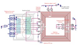
The CMOS PA circuitry now includes four power cells and the IPD transformer, and this was driven differentially at the input using a balun and matching inductor. This combination yields drain efficiency that is close to the load-pull result, but with a drop in amplifier PAE due to the IPD pre-match inductor.
To house this PA circuitry, a standard 4 x 4 mm QFN package from Amkor was selected, with the addition of three-dimensional (3D) bond wires to model the mutual inductance and provide a means for optimization. Since the structures are differential, adding the mutual coupling of the bond wires shifted the results. Once again, the “rapidly added complexity” methodology was applied to understand and address the problem. In this case, the bond wire height and proximity were adjusted to minimize the coupling (Fig. 7).
For the CMOS-based PA design, along with optimizing Pout and PAE, it will be necessary to consider the voltage swing across the devices’ worst-case high Vbatt battery-voltage conditions for reliability reasons. The voltage swings that were achieved in the CMOS design are barely acceptable; additional steps should be taken to mitigate that voltage swing by clamping or regulating the control voltage. To evaluate the CMOS technology mix at the package level, the inductors and transformer were chosen as separate and optimizable.
The PA based on the CMOS technology mix is very different compared to the GaAs-based design. It offers numerous advantages, being simple and compact, with integrated power control and all matching realized on the IPD. But it also has disadvantages, with the discrete transformer limiting the number of stacked active devices in the cascode, limited impedance tunability with the transformer, and with PAE somewhat degraded by the use of the pre-match inductor.
By completing two functioning designs, it is possible to realistically compare the two technology mixes and how they might serve different applications. The insights gained at this level are far more meaningful and invaluable than a simple device-level comparison of technologies. This methodology makes it possible to compare two different technology mixes in weeks or even days, eliminating the risk associated with choosing a poor technology mix. The capability to move up and down levels while rapidly adding complexity with an iterative design approach provides a great deal of insight into how the different technology mixes will perform in the final product designs.
It should be noted that to implement this design methodology, the following are required: access to different technologies and PDKs, integrated EM simulation technology, parameterizable and optimizable physical layout for circuits, and the capability to analyze performance with modulated signals. The use of this “rapidly added complexity” methodology is broadly applicable and can help reduce risk early in the design process, as well as eliminate problems and speed time to market.
Editor’s Note: Readers seeking additional information on this GaAs versus CMOS technology comparison, including Advanced Design System (ADS) model files for both CMOS and GaAs PA module designs, are invited to visit Agilent Technologies’ page on the topic.
Matthew Ozalas, RF Power Amplifier Designer
Agilent Technologies, Agilent EEsof, 5301 Stevens Creek Blvd., Santa Clara, CA 95051; 408-345-8886, FAX: (408) 345-8474.
This file type includes high resolution graphics and schematics when applicable.
