Evaluate EDA Software For A Wireless World
This file type includes high resolution graphics and schematics when applicable.
Engineering design and analysis (EDA) software has evolved into an essential tool for wireless circuit and system design. High-frequency engineers are now using RF/microwave EDA software tools to achieve effective and efficient design flows for a wide range of circuits and systems, in commercial, industrial, and military markets. In addition, engineers now rely on EDA software tools to shorten the product design cycles significantly for many different circuits and systems.
Although EDA software tools have been in use for many years, early EDA tools have not always been central to the process of creating circuits. EDA software has been available, in one form or another, almost since the early days of computers. Even when available, however, the software was often cumbersome to use. Most early circuit designs were performed with a pencil and a slide rule.
In the early days of simulation software, computer programs such as SPICE and ECAP were the only available EDA tools. SPICE was developed at the University of California at Berkeley and made available to the public in the mid-1970s. SPICE included nonlinear analysis in the time domain, but not transmission lines or scattering (S) parameters. It was not very useful for RF or microwave work. The latest version of SPICE, Spice3, is still supported and available along with user manuals from the University of California at Berkeley website. The ECAP software contained no transistor models (the user had to generate their own models and create a netlist for them), and it could not handle noise or nonlinearity.
By the 1970s, computers had evolved sufficiently to allow for improved EDA software capabilities. One catalyst was the PDP series of VAX computers from Digital Equipment Corp. (DEC). These “mini-computers” as they were known, occupied the space of a large office and provided more sophisticated functionality, eventually including integrated-circuit (IC) layout capabilities. These computers and their processing power levels were a huge step in the direction of improved EDA capabilities.
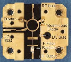
Changes in high-frequency technologies were a second factor in the development of EDA software. Before 1960, virtually all microwave components were realized in waveguide or machined transmission-line structures. In the 1970s and 80s, microwave hybrids on both hard and soft substrates became much more common, but the development process involved an approximate design and lots of manual “tweaking.” Software tools appropriate to this kind of design were developed; one of the most important was COMPACT. It ran originally on mainframe computers with a timesharing system, and later on DEC VAX machines. Figure 1 shows a hybrid circuit developed with aid from software of this era: a 1980s-era, 30-GHz mixer hybrid realized on a fused-silica substrate. Individual pieces of the circuit were designed using the EDA software of the day, but the circuit as a whole was not simulated. Layout was performed by a technician who received a dimensioned drawing (which, fortunately in this case, was error-free).
As hybrid technology evolved into increased use of ICs, it became evident that the “build-and-tweak” approach would not be adequate. It was obviously impossible for ICs, but even for hybrids, the cost in development time was increasingly becoming a burden. The problem was not so much the circuit analysis as the circuit-element modeling. Such elements as microstrip step and tee discontinuities were not well characterized, and these structures had profound effects on high-frequency circuits. Precise design was usually impossible.
This file type includes high resolution graphics and schematics when applicable.
Era Of Integration
This file type includes high resolution graphics and schematics when applicable.
The lack of integration between EDA products contributed to a poor design flow, the process of moving a design from concept to realization. Generally, the design flow consisted of an electrical design, which was turned over to a layout technician, who then created an IC or hybrid layout in graphics software. At that point, a problem in the design was often discovered (such as a component or circuit structure that didn’t fit the layout) and redesign was necessary. It was not unusual to have several design iterations through layout and circuit simulation before a design was complete. This process was slow, error-prone, and expensive.
The fundamental problem was that most EDA products were “point tools”: individual software products that performed a single type of analysis, such as circuit simulation, electromagnetic (EM) analysis, system simulation, or layout. Much of an engineer’s design time was spent operating these disparate tools and shuffling data back and forth between them, and it was difficult to identify, for example, a layout problem or an EM simulation error early in the design cycle. The obvious solution was to integrate point tools so that layout, EM analysis, and system simulation could be performed concurrently with the electrical design.
Early attempts to integrate EDA products involved creating a “framework,” a supervisory program that operated all the products and moved data between them. Because of the great differences between the point tools, however, the results were often clumsy, technically limited, and buggy. Much of that clumsiness was the inevitable result of the need to integrate products that had never been intended to work together.
The best way to ensure interoperability is for those products to be designed together from the start. By the time the need for integration became critical, however, existing EDA products had become big and complex, and redesigning them was a job too large for the makers to contemplate. New products began with a clean slate, however, and achieved much smoother integration. Additionally, new technologies, such as object-oriented design and Microsoft’s Component Object Model (COM) technology, allowed greater versatility and interoperability between software modules. This assured the greater integration and interoperability that is the hallmark of modern software design.
Modern Design Flow
In the past, the computational speed of EDA software was essentially viewed as the single characteristic of interest. That is easy to understand, as the limitations of both computers and software systems meant that many kinds of analyses, especially EM simulations, were painfully slow. As computer and software capabilities improved, however, it became clear that the design-flow bottleneck was the dominant factor in development time. Accordingly, it affected not only the cost of design but the time to market. As the RF/microwave world moved more toward commercial products and away from government and military development, long time–to-market costs meant lost opportunities. The cost of that loss was far greater than the direct costs of circuit and system development.
Achievement of a faster design process does not involve the mindless pursuit of software processing speed; it results from smoothing the design flow. This, in turn, requires attention to the software design of the entire system, not just the software simulator tools. The goal is to perform electrical design, EM design, and layout concurrently, so that iterations between all of these functions can be avoided. This capability smooths the design flow enormously and decreases costs dramatically.
A number of different simulation system characteristics contribute to the effectiveness of a modern design flow, including accurate EM models, tight integration between EM and circuit simulators, tight integration with system simulators, layout and circuit interoperability, and advanced graphics capabilities. EM simulators, as invaluable as they can be, still have a strong impact on the time needed to complete a design. The use of even a high-speed EM simulator for for every microstrip step and T-junction is a waste of time. It makes more sense to analyze such structures beforehand, store the results in tables of data, and interpolate them when needed.
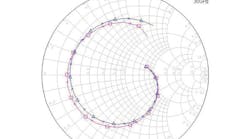
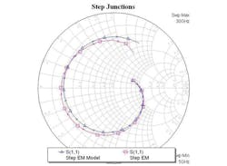
Discontinuity models realized in this manner, containing a database of EM results, are fast and accurate. Figure 2 shows the S11 response of a large step junction plus microstrip interconnects using an EM model and a full EM simulation. It’s clear that the EM model is insignificantly different from the full EM simulation, diverging only at frequencies where the 25-mil alumina substrate would be inappropriate anyway (because of spurious modes).
This file type includes high resolution graphics and schematics when applicable.
EM Simulation Revisited
This file type includes high resolution graphics and schematics when applicable.
During the “dark ages” of EM simulation, it was necessary to redraw the structure for the EM simulator and to transfer EM-generated S-parameters back into the circuit simulator manually. This process led to many opportunities for errors. Modern simulators treat an EM-simulated structure directly as a circuit-simulator element that is then analyzed in a manner no different from any other S-parameter block. No copying or redrawing is necessary and, in fact, the EM structure is copied directly into the layout tool as well. This prevents “translational” errors or unnecessary, time-consuming repeated effort.
EM simulation is not just for microwave circuits. For example, in a cellular handset power amplifier, the load impedance is only a few ohms. Even at 1800 MHz, the inductance of the chip’s output bond wires cannot be ignored, as it is a large fraction of this value. EM simulation is really the only accurate way to predict that inductance at design time. EM simulation is also useful for finding areas of dangerously high current density or, in high-power circuits, high-field regions that could lead to arcing.
In the days when most high-frequency design was performed in the aerospace industry, system simulation was largely divorced from the circuit-design process. In wireless systems, for example, individual circuits can have strong effects on system performance, so system design must be concurrent with circuit design. This is especially true for power amplifiers, where amplifier nonlinearities must be carefully monitored to meet adjacent-channel-power (ACPR) specifications. Tight integration between circuit and system simulators, in which a circuit from the circuit simulator can be treated automatically as a block in the system simulator, can be an enormous aid to the design process.
In a modern EDA system, each circuit element has a single representation in the EM, layout, system, and circuit simulators. Because it has only one instance in the simulation system, changes in its circuit parameters are immediately reflected in the layout. Similarly, changes in the layout, such as a change in microstrip line length or width, are immediately seen in the circuit simulator. No “back-annotation” or other such processes are needed, and the need for layout-versus-schematic (LVS) checking is greatly reduced. In this way, a designer sees the consequences of a change immediately and can modify the circuit if something is not practically realizable. And indeed, this is how it should be: Layout is part of the engineering design and should not be off-loaded onto a layout technician.
Advanced Layout Views
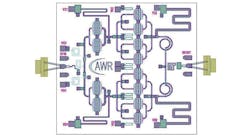
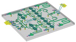
A graphics system used for circuit layout must be clear and easy to follow. Visual fatigue and lack of clarity lead to errors. Computers are now available with powerful graphics capabilities, and it makes sense to put such capabilities to use as part of the RF/microwave design process. Figure 3 shows an example of a circuit layout of a power-amplifier chip, showing the clarity and detail possible. Figure 4 shows a three-dimensional (3D) view of the layout, which can be rotated in all axes. Such graphic capabilities are invaluable in ensuring that a high-frequency layout is created as intended.
EDA tools have come a long way in the past few decades. They have evolved from individual tools with limited functions to systems that provide more accurate designs, smooth the design flow, and greatly reduce design costs. These advantages come from the use of modern software technology as well as improved technical capabilities. Evolving products, such as Virtual System Simulator (VSS) from AWR, make it easy to move from system-level design and behavioral modeling to detailed component-level design and ultimately performance evaluation. Today’s EDA systems are powerful and versatile, and a huge advantage over those of even the recent past.
Dr. Stephen Maas, Chief Scientist
AWR Corp., a National Instruments Co., 1960 East Grand Ave., El Segundo, CA 90245; (310) 726-3000.
This file type includes high resolution graphics and schematics when applicable.
