Load-Pull Methods Yield Improved Base-Station PAs
Download this article in .PDF format
This file type includes high-resolution graphics and schematics when applicable.
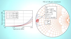
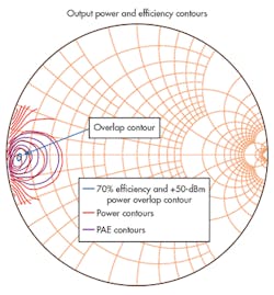
Load-pull measurements are a powerful aid in identifying impedance matches for RF/microwave components. In a load-pull simulation of an active device, the impedances presented to the source and load of the device are swept across a range of values, and the effects on performance are measured. The performance contours are then plotted on a Smith chart (Fig. 1) to show how the changes in impedance impact device performance. By knowing how active-device performance is related to the input and output impedance of a power amplifier (PA), for example, key attributes such as output power and linearity can be fine-tuned for optimum performance.
The capability to import and manipulate these load-pull data sets in an electronic-design-automation (EDA) circuit-simulator software program greatly simplifies and speeds the design process. It also gives designers a broader design space to explore the performance impact of different design options.
EDA software tools such as the NI AWR Design Environment V12 from National Instruments enables designers to take full advantage of these new load-pull file features in an intuitive manner by offering important load-pull measurements and graphing control. To address the high-performance requirements of PAs used in modern wireless communications working with analysis of swept input power, the NI AWR software V12 load-pull capability supports studying amplifier responses to input power sweeps. However, it also allows any design parameter to be swept and the data manipulated in the design environment.
Traditional Design Flow
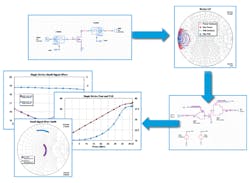
A traditional circuit design flow for a PA typically involves developing a nonlinear model of the active device to be used in a design circuit, and then performing a load-pull simulation of the device model in a commercial circuit-simulation program (Fig. 2). The input and output impedance-matching networks are then designed based on load-pull contours. The idea is to find a terminating impedance that will yield performance criteria most important for realizing system requirements. By comparing the simulated results with the design results, a circuit designer can readily adjust the matching network to achieve the performance goals or optimized performance levels for that particular device model.
Creating accurate nonlinear device models absorbs a considerable amount of time, effort, and expertise in active device characterization. The process often requires a significant investment in measurement equipment and large-signal modeling/optimization routines, which must continually evolve to keep up with changes in technology. As a result, it’s difficult to collect enough test data to create a nonlinear device model that predicts the performance of an active device under all operating conditions, such as bias point, frequency, and power level.
Designing for such a broad and dynamic set of operating conditions is a growing concern among designers faced with developing PAs used in modern communications systems. In addition, nonlinear-device-model development is a timely process, requiring multiple cycles of measurement and model extraction, curve fitting, and model optimization, further cutting into the short design cycle time typically associated with wireless devices and underlying PA components.
To circumvent the dependence on active-device nonlinear models, PA designers have begun designing impedance-matching networks and associated circuitry based directly on measured load-pull data for a device of interest. This offers several advantages compared to the traditional PA design flow. For instance, the entire design process is within the control of a design group—there is no reliance on a nonlinear device model developed from an outside source and outside measurements. Device data can be regenerated or redefined in-house if necessary, rather than relying on a third-party source for nonlinear active-device-model generation.
Grappling with the Complexity
The challenge for EDA software companies is to provide a manageable and intuitive way for dealing with complex, swept load-pull data sets. These data sets can include nested harmonic load-pull data, nested load- and source-pull data, and two-tone excitation data, in which intermodulation-distortion (IMD) levels can be studied as a function of load impedance. The data can also include multiple fundamental frequencies.
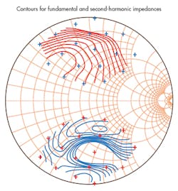
As such, an entire array of possibilities exists for manipulating the data, including plotting circuit performance as a function of frequency, power, bias, load impedance, or source impedance at a fundamental frequency of interest, and the results of changing load or source impedance at harmonic frequencies. Figure 3 shows an example of data plotting and manipulation of contours for impedances at fundamental and second-harmonic frequencies. Managing all of this information for use by the PA designer requires support from software automation.
Above and beyond viewing and plotting swept load-pull data, the capability to directly determine matching network source and load impedances to achieve optimal PA performance is of paramount importance. Matching networks that are designed from measured load-pull data enable fast and accurate assembly of PA circuit prototypes. That’s because the uncertainty of a nonlinear model is removed and replaced with verifiable data, which can be easily obtained through measurement for the specific operating conditions under consideration. In this way, once the load-pull data have been imported into a circuit design software simulator, the matching networks can be designed directly using the EDA software and its built-in matching network utilities and harmonic balance analysis (for frequency-domain, nonlinear simulations).
Another requirement for the design software is the ability to produce data sets that are equivalent to the measurement-based data used to develop the nonlinear models. Fitting simulation results to empirical data is required for modeling teams to verify the accuracy of their nonlinear device models. Therefore, the circuit design software must be able to produce equivalent measurements within the software, including more complex measurements such as adjacent channel power and intermodulation distortion. In this way, the circuit simulator is used not only for data manipulation and circuit design, but also for improving the accuracy of nonlinear device models.
Load-Pull Design Environment
Historically, single-sweep point files have been supported by commercial load-pull system suppliers (LP/SP files from Maury Microwave and LPD files from Focus Microwaves). NI AWR Design Environment V12 software now supports multidimensional load-pull files such as Maury’s SPL and CST files and Focus’s LPD files, based on swept data. Files with more extended data sets, such as multiple gamma points, frequencies, and power steps, give NI AWR V12 software the opportunity to execute more seamless, intuitive post-processing of data with more comprehensive results in terms of PA design (Fig. 4).
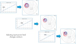
The new load-pull formats in the NI AWR Design Environment, specifically Microwave Office circuit design software, offer circuit designers access to an extensive array of data-manipulation functions. Figure 5 shows a rectangular graph of input power versus the index on the left. A marker points to a specific input-power level, with the contours for that power level plotted on the right. When the marker is moved, another set of contours will be shown corresponding to that power level. If the marker is moved again, a third set of contours is obtained, and so on, providing designers with multiple views of critical aspects of a PA circuit design’s behavior—a much more comprehensive analysis tool than possible with older single-point local files.
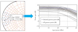
Conversely, instead of choosing an input power level and plotting contours, users can select a gamma point or impedance value and plot swept data for that data point. Figure 6 shows how gain-compression curves can be plotted by choosing a gamma point from the impedances in a data file. The plots in Fig. 6 show both gain-compression curves for all gamma points in the file as well as the gain-compression behavior for a gamma point selected with the marker.
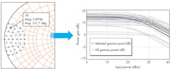
If the marker is moved to another gamma point, the gain-compression curve changes to reflect the performance at the new impedance (Fig. 7). This feature highlights the tradeoffs in gain compression as a function of load for the entire swept input power range, enabling designers to quickly choose the load necessary for optimum gain-compression behavior given an expected input power.
New Design Flows
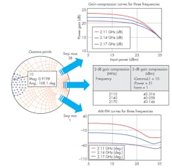
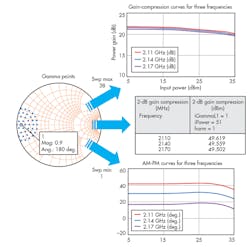
The new load-pull analysis capabilities in this latest version of the NI AWR Design Environment (V12) make it possible to develop a new design flow for base-station PAs and other active circuits. As an example, Figure 8 shows impedance points plotted for a 2.1-GHz active device, a silicon, laterally diffused, metal-oxide-semiconductor (Si LDMOS) transistor, capable of 80-W output power at 1-dB compression (P1dB). A gamma point was chosen and the AM-to-PM and gain-compression curves were plotted for three frequencies in the file (2.11, 2.14, and 2.17 GHz). The 2-dB gain-compression output power was also computed and plotted in tabular format.
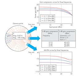
Figure 9 shows how users can move a marker to select different gamma points and parse through the performance possibilities of a device, assessing tradeoffs at different points. If another impedance point is chosen, a new set of performance curves is automatically generated, corresponding to that new load impedance, as well as another set of AM-to-PM-conversion and gain-compression curves and another 2-dB gain-compression output-power value.
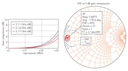
As an example, Figure 12 shows three curves for gain compression increasing to about 6 dB at three different frequencies. A center band at 2.14 GHz and 3-dB compression point were chosen for analysis. With this software simulation functionality, the contours can be plotted for any desired performance parameters. In the case of Fig. 12, contours are plotted for output power and PAE, two likely parameters of interest for designers of cellular base-station PAs.
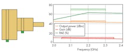
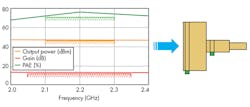
With the new EDA software package, impedance-matching networks can be optimized directly from the load-pull data. In Figure 13, output power, gain, and PAE are plotted, this time as functions of frequency. The impedance-matching networks can now be tuned or optimized based directly on achieving the best possible results for all three of those performance parameters. Obviously, the highest value for each parameter may not occur at the same impedance points. But having the capability to show simulations of performance parameters as functions of impedance values helps avoid the endless loop of trying to find the highest possible performance levels for one parameter, while not degrading the performance level of another parameter below an acceptable value.
Furthermore, the enhanced load-pull capabilities enable users to tune directly, or optimize using a wide variety of included optimization algorithms. The bars in the Fig. 12 establish goals for a designer seeking to optimize a circuit. Once goals are set, the optimization runs on the matching network to meet the desired performance, which in turn updates the physical parameters for the matching network.
Figure 14 shows the result of the optimization and the updated matching network. The goals can easily be modified to further optimize the design, and the matching network parameters will be updated based on the optimization result. This capability to optimize directly from the local performance data file itself is a very powerful concept.
For an empirical-based design, load-pull functionality has lowered dependency on third-party nonlinear models and provided increased control of the design process for an engineering team. Designers can perform additional load-pull measurements on an active device as needed to “feed” the EDA software, rather than waiting for the creation of a new nonlinear device model. With a software tool like NI AWR Design Environment and its design flexibility, load-pull data can yield not only improved performance of PAs for base stations, but shorter times to market that are often critical in competitive marketplaces.
Looking for parts? Go to Parts Direct.
