This file type includes high resolution graphics and schematics when applicable.
Predicting the outcome of advanced processes, such as those for fabricating semiconductors or microelectromechanical-systems (MEMS) devices, can be extremely complex. The calculations are not made any easier as device features continue to shrink in size. However, a new three-dimensional (3D) simulator from Coventor, SEMulator3D, has proved capable of performing like a virtual foundry.
SEMulator3D helps evaluate new semiconductor or MEMS designs before performing expensive experiments with a foundry process. The recently announced sixth generation of this modeling tool builds on previous versions by combining structural modeling with sophisticated electrical analysis capabilities; adding new features; and allowing users to expand the program at any time with an add-on software module for resistance and capacitance parameter extraction.
The sixth-generation SEMulator3D process simulation software adds new features and analysis capabilities, including resistance and capacitance solvers, but maintains its ease of use thanks to a straightforward GUI.
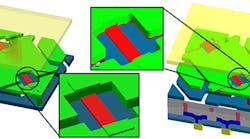
Variations exist within any electronic semiconductor material, no matter the wafer size. Further variations occur with each process step used to fabricate a MEMS device or semiconductor, such as a field-effect transistor (FET). The SEMulator3D 6.0 software (see figure) uses physics and 3D voxel (cube-based) modeling technology to analyze device structures and predict the outcomes of complete process flows for analog and digital devices.
In the world of 3D imaging, a voxel or volume element is a type of building block, like a pixel in a two-dimensional (2D) environment. SEMulator3D also features surface-evolution modeling that predicts the effects of changes in surface features during different process steps.
This physics-based software evaluates device design and fabrication as a function of the process flow, analyzing a semiconductor or MEMS fabrication process as a series of unit process steps that can be understood and optimized. Typical fabrication steps involve different types of etching; deposition of layers; epitaxial and other means of growth; and functions such as lithography, implantation, and diffusion.
A user can enter geometrical and physical parameters for each process step to experiment with known or unknown process variations and to better understand how the different device process steps interact with each other when producing the final device. The software helps analyze a wide array of devices, including NAND flash memory, DRAM, FinFETs, nanowires, and MEMS devices.
What Functionality Was Added?
This latest software version allows for random insertion and placement of defects as part of enhanced process diagnostics. In this way, a user can trace a known defect back to an originating process step or the tool that might have caused it. The new version also enables users to export meshes to additional file formats, as might be needed for analyzing dopant concentrations in a 3D finite-element-analysis (FEA) software program.
Perhaps one of the strongest new capabilities of this sixth-generation software is the SEMulator3D Electrical Analysis module. It allows users to better understand how device and process variations translate into resistance and capacitance effects for a given design. The software solves for resistances and capacitances without requiring time-consuming meshing or data export to mathematical analysis tools.
David Fried, chief technical officer, semiconductors, for Coventor explains, “Now, our users can link the process variations in the fab and the design choices of the product to real electrical impact, through process-predictive structural modeling and our more advanced Electrical Analysis tool.”
In spite of its sophistication, the software is easy to use thanks to a straightforward graphical user interface (GUI). Ease-of-use was further enhanced for SEMulator3D version 6.0 through a new environment for the Analysis Editor. Analysis steps—e.g., metrology, structure search, and parasitic extraction—are now separated from the process sequence for to make it easier to apply input data and understand the results of modifications. The simulation software can also import design data as GDSII layout data or OASIS layouts, or operate on post-OPC design data.
In addition to achieving its sixth generation of an advanced process modeling tool, the firm offers a number of variations of the software that may provide solutions for users with disparate needs. The base virtual fabrication software offers the means for visualizing various ion implantations, dopant concentrations, epitaxial processes, etching, and DSA processes as part of fabricating a device or an IC. Additional modules include (but are not limited to) the new SEMulator3D Electrical Analysis bundle, which can calculate the resistance of conductor nets and the capacitance between nets directly within SEMulator3D.
Coventor Inc., 1000 Centregreen Way, Ste. 200, Cary, NC 27513; (919) 854-7500
This file type includes high resolution graphics and schematics when applicable.


