Create Robust UHF RFID Tag Antennas on Dielectric Substrates
Download this article in PDF format.
Ultra-high-frequency (UHF) radio-frequency identification (RFID) tag antennas, commonly used for inventory and tracking, need to be inexpensive, compact, and robust for the environment in which they will be installed. New antenna synthesis tools have proven very effective in the design of antennas for a wide variety of applications. Now these tools are being applied to overcome the challenges of designing RFID tag antennas.
This article describes how the AntSyn antenna synthesis and optimization tool, along with the NI AWR Design Environment, are employed to combat these challenges. It also presents an example RFID tag antenna created with this technology.
RFID Tag Antenna Design Issues
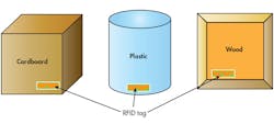
The design and integration of RFID tag antennas in the real world can be difficult when trying to make them environmentally immune to the mounting platform. This is especially the case when installing them over a dielectric, as the underlying dielectric properties are likely to be highly variable. A single tag design may be used, for instance, on cardboard, drywall, plastic, fiberglass, wood, or other dielectrics1(Fig. 1).
Designing a broadband response is a common approach to ensuring that antenna performance is maintained over a variety of dielectric substrates, each of which will shift the resonant frequency.2-4 However, to support integration on a wide variety of objects while reducing costs, RFID tag antennas also need to be compact. Unfortunately, when an antenna is made smaller compared to wavelength, the bandwidth narrows,5 and thus becomes much more sensitive and difficult to design.
In addition, while antennas are usually designed to match a real (typically 50 â¦) standard line impedance, the RFID chips themselves are generally not 50-⦠devices and have reactive impedances. A typical value for a chip impedance might be 16 – j148 â¦.2
To minimize reflection losses, it is desirable to directly design the antenna impedance to be a conjugate match of the RFID chip’s complex impedance. Therefore, a matching network will not be necessary. Direct antenna-to-chip matching will significantly decrease the cost and complexity, as well as improve the overall reliability. However, this non-standard impedance matching makes the design challenge even more complex.
The various approaches2-4 used in prior research to meet the challenges associated with designing RFID tag antennas have employed human-in-the-loop engineering methods. Designing and optimizing such antennas by hand is a time-consuming and difficult process, and electromagnetic (EM) tools generally offer limited ability to explore the design space beyond modest tweaking of the antenna’s geometry through parameterization. Furthermore, limited design space optimization is particularly restrictive when making an environmentally robust antenna.
AntSyn antenna synthesis software, on the other hand, has proven its effectiveness at efficiently creating many different types of antennas,6,7 and is now being used to overcome RFID tag antenna design issues. It supports the simultaneous optimization of RFID antennas directly to chip impedance on an array of user-specified dielectric substrates.
Automated Synthesis Design Approach
AntSyn software uses evolutionary algorithms (EAs), a programmatic method that leverages EM simulations to efficiently explore the design space and automatically locate high-performance design options. Users are able to enter RF and form-factor specifications such as bands, patterns, efficiency, geometry constraints, and more. It maintains a library of design templates and takes advantage of a full-wave 3D EM simulation8 solution to obtain performance information on candidate designs. Advanced algorithms are employed to select and create antennas that are optimized to meet user requirements.
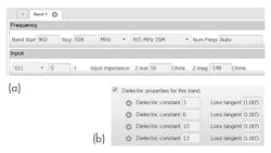
The AntSyn band control option enables the user to select many different performance criteria generally related to frequency bands, such as start and stop frequencies, pattern requirements, polarization, and cross-polarization levels. AntSyn also makes it possible to specify a complex input impedance and multiple dielectric properties to be simultaneously optimized for the specified frequency band (Fig. 2). During optimization, antenna performance is evaluated on each of the specified dielectrics.
Another antenna type in the AntSyn library enables environmentally immune design, using a generic XY-mesh type antenna. The antenna is a single-layer, connected XY-mesh design on a dielectric substrate. Since the substrate is utilized to simulate the surface on which the RFID antenna will be installed, it provides fixed user-specified dimensions relative to the antenna rather than being optimized as part of the antenna. Antenna dimensions are limited by the user-specified geometry control.
RFID Application Example
AntSyn was used to synthesize an RFID tag antenna matched to four dielectric substrates and a complex chip impedance. The specifications shown in Fig. 2 were applied, in addition to the following “box” geometry limits: X = 4 in., Y = 1 in., and Z = 0.25 in. A 2-mm substrate thickness was used, as in Ref. 2. It took only a few minutes to set up the specifications, and then the run was executed. Edging of the mesh was used to increase the accuracy of the simulation at the expense of a longer simulation run time.
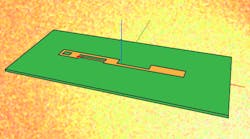
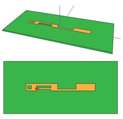
The resulting antenna design features a single metallic layer (gold) on a dielectric (green) (Fig. 3). The red dot indicates the chip position. The antenna dimensions are 100.5 × 9.6 mm (3.96 × 0.38 in.), while the overall substrate measures 167.1 × 76.1 × 2 mm.
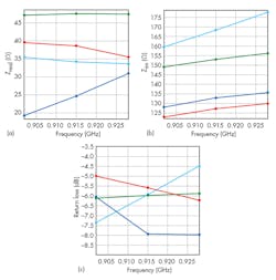
The input impedance and return loss (matching of the conjugate antenna impedance to the chip impedance) for this antenna are shown in Figure 4. According to Ref. 2, a coupling of –2 dB appears to be acceptable; the synthesized antenna is well below this specification over the desired frequency band of 902 to 928 MHz.
Conclusion
Thanks to new capabilities in antenna synthesis tools, such as AntSyn, antenna designers can successfully and efficiently overcome challenges in designing RFID tag antennas and meet requirements for low cost, small footprint, and robustness to the installation environment. The example provided in this article illustrates that it is possible to automatically synthesize a compact antenna that works on multiple substrates and directly matches chip impedance. These new tools can be used for many other applications beyond RFID antenna design, such as to increase yield for antennas that are sensitive to dielectrics or for body-worn or body-internal antenna design.
Derek S. Linden is Director of Technology, and Jennifer Rayno is Senior Development Engineer, at AWR Group, National Instruments.
References
1. Gaetano Marrocco, "The Art of UHF RFID Antenna Design: Impedance-Matching and Size-Reduction Techniques," IEEE Antennas and Propagation Magazine, Vol. 50, No. 1, February 2008, pp.66-79.
2. Shuai Shao, Robert J. Burkholder, and John L. Volakis, "Design Approach for Robust UHF RFID Tag Antennas Mounted on a Plurality of Dielectric Surfaces," IEEE Antennas and Propagation Magazine, Vol. 56, No. 5, October 2014, pp 158-166.
3. T. DeJeruyelle, P. Pannier, M. EgeJs, and E. Bergeret, “An RFID Tag Antenna Tolerant to Mounting on Materials,” IEEE Antennas and Propagation Magazine, Vol. 52, No. 4, pp 14-19, August 2010.
4. Jun Zhang and Yunliang Long, "A Dual-Layer Broadband Compact UHF RFID Tag Antenna for Platform Tolerant Application," IEEE Transactions on Antennas and Propagation, Vol. 61, No. 9, pp. 4447-4455, September 2013.
5. R. F. Harrington (1960). "Effects of antenna size on gain, bandwidth, and efficiency." Jour. Nat'l Bureau of Standards. Washington D.C., USA: US National Bureau of Standards. 64–D: 1–12.
6. Jason D. Lohn, Derek S. Linden, Bruce Blevins, Thomas Greenling, and Mark R. Allard, “Automated Synthesis of a Lunar Satellite Antenna System,” IEEE Transactions on Antennas and Propagation, vol 63, no 4, pp.1436-1444, April 2015.
7. http://hothardware.com/news/3d-systems-3d-printing-with-conductive-ink-for-project-ara-antennas
8. WIPL-D Pro v11.0, Software and User’s Manual, WIPL-D d.o.o., Belgrade, 2014.
