Dive into EM/Circuit Co-Simulation of a T/R Front-End Module and Actively-Scanned Array, Part 1
Download this article as a .PDF
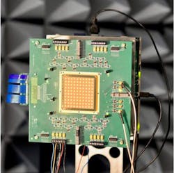
5G is poised to bring more integrated and sophisticated antenna and circuit modules to the modern defense and commercial electronics markets. For example, Fig. 1 shows the type of antenna module that is now being prototyped by manufacturers like IBM and Ericsson.1 This 28-GHz 5G antenna module is a 2.8 × 2.8 in, 8 × 8 patch array with 64-dual polarized elements and four monolithic microwave integrated circuits (MMICs) using a silicon-germanium (SiGe) process.
1. Shown is a 2.8-×-2.8 in. 28-GHz 5G antenna module with integration of multiple technologies.
Other proposals in the design community use a combination of silicon and gallium-arsenide (GaAs)/gallium-nitride (GaN) technologies. The advantages of these types of modules are lower cost, smaller size, integration of multiple technologies, and ease of deployment.
This article, part 1 of a two-part series, examines today’s multi-technology circuit and electromagnetic (EM) simulation challenges and the software tools that are needed to support the successful design of 5G products. Part 2 presents examples that illustrate the use of multi-technology in an EM simulation and EM/circuit co-simulation of an actively-scanned antenna array. Advanced technologies, such as parameterized 3D cells, shape pre-processing and simplification, 3D EM extraction, and in-situ measurements, are described.
Multi-Technology Circuit and EM Simulation Challenges
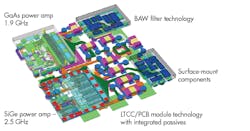
Designers of 5G products need RF/microwave software tools that enable them to work with multiple technologies integrated into one module, such as the dual-band transmit/receive (T/R) prototype module shown in Fig. 2. This wireless local area network (WLAN) module incorporates many different technologies integrated together, such as a GaAs power amplifier (PA), a SiGe PA (because much of the control electronics will be silicon), various surface-mount components, bulk-acoustic-wave (BAW)/surface-acoustic-wave (SAW) filters (very popular for mobile technology), and low-temperature co-fired ceramic (LTCC)/printed-circuit-board (PCB) technology with integrated passives. To support this type of design, the software design environment must overcome two big challenges.
2. This figure illustrates a T/R dual-band WLAN module with many integrated technologies, which will connect to an antenna array.
Different Physical Technologies
5G designers will need to use several different physical technologies (such as GaN, GaAs, ceramic, and silicon for the chips), as well as various board and module technologies (for example, low-loss organic materials for the boards and ceramics for the modules). The EM simulator must support these multiple technologies (commonly called multi-technologies) by being able to use multiple libraries or process design kits (PDKs). These different technologies will exist in the same EM simulation if the geometry is a transition region between a chip and a module. The simulation environment must therefore support co-existence of libraries in the same project.
Different EM and Circuit Simulators
Different EM and circuit simulators will also be required, depending on the specific geometry and desired information. The software needs to support time-domain, frequency-domain, and more complex modulation-domain circuit simulators. In the time domain, SPICE-like simulators for SPICE-based models, silicon chips, and interconnect lumped parasitic nets will be needed.
Frequency domain (harmonic balance) will be needed for RF simulation of PAs and filters. Multi-technology designs will require a modulation domain for complex coding schemes, such as LTE, in which the carrier is deeply modulated and not periodic. Using simply SPICE or harmonic balance will not be sufficient, and designers are now moving towards more sophisticated hybrid simulation methods that the software will need to support.
Different EM simulation technologies are required, depending on the geometry being simulated. Planar EM simulators have higher capacity and speed for traditional planar-type layouts on PCBs and chips. For example, planar distributed filters, PA distribution manifolds, and interconnects on the board or chip are usually simulated with planar EM simulators. 3D simulators are required for transition regions between different technologies—for example, between a board and ball-grid array (BGA) module, or a module and a chip using bond wires.
Multi-Technology Design in EM
EM is one of the bigger challenges in multi-technology design, mainly because more than one manufacturing technology is being used. For example, transitions between a chip on a board or a module and a chip involve multiple technologies. This requires two or more libraries (commonly called PDKs) for the various board, module, and chip technologies being used. Each library has a different stackup, artwork cells, and design rule checks (DRCs).
Using multiple libraries for different EM simulators also has complications because the stackup information can be different; material properties and ports and boundaries can be treated in different ways; and there are different simulation settings, such as solver accuracy and frequency ranges for each simulator. Drawing and layout creation is also a problem, since 3D and planar layouts typically have differences in their construction.
NI AWR Design Environment software offers a unique EM Socket technology that provides one unified environment for controlling multiple EM simulators. These simulators include AXIEM planar and Analyst 3D finite-element method software, as well as third-party EM tools. Figure 3 illustrates the AWR Connected for ANSYS HFSS that integrates HFSS with NI AWR software. Most of the layout is created in the AXIEM planar EM simulator shown on the left. HFSS is then selected as the EM simulator (middle). The resulting HFSS dataset is imported back into Microwave Office circuit design software to tune, optimize, perform yield analysis, and verify results (right).
3. EM Socket allows users to take advantage of third-party EM tools. Shown here is AWR Connected for HFSS.
NI AWR Design Environment addresses the issue of using of both a 3D and a planar simulator in the same design by assuming chips, boards, and modules are essentially planar layouts with 3D “islands.” While designers cannot draw 3D arbitrary shapes in a planar environment, they can import 3D shapes from a library of pre-drawn standard cells such as BGAs, bond wires, SMA connectors, and more.
A full 3D editor interfaces with the design environment if needed. Library (PDK) support for multiple technologies in NI AWR Design Environment is available for both the Microwave Office circuit simulator, where models from the different PDKs are used, and the EM simulators, where the artwork cells, materials, and stackup properties of the various PDKs are available.
Hierarchy Technology
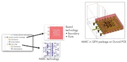
Hierarchy technology is available within Microwave Office to enable and organize the use of multiple PDKs (Fig. 4). Designers can use different technologies at the same time by assigning a technology to each layout cell. Different layouts/technologies can then be embedded within one another as cells and sub cells. Ports and boundaries are added at the highest level of hierarchy. The final layout is then flattened into a single layout and sent to the EM simulator. Clearly, a 3D EM simulator such as Analyst makes the most sense for multi-technology layouts.
4. Shown is a multi-technology layout of a MMIC in a QFN package on a Duroid PCB. Three technologies are employed.
Conclusion
Complex 5G and radar infrastructure requires the integration of antennas and circuitry. The challenge for EDA software is to support multiple technologies that require different circuit and EM simulators. Hierarchy at both the circuit simulation and EM level can be used to control multi-technology designs. Part 2 of this article will discuss EM/circuit co-simulation for antenna and circuit interactions, which can be modeled with in-situ simulation.


