Software Tools Bring a Unique Approach to Filter Design
Download this article in PDF format.
No question, the task of designing high-frequency filters can be made much easier by taking advantage of the capabilities of today’s design software tools. Whatever the filter, whether lumped-element, distributed, cavity, or some other kind, simulation software is readily available to help do the job at hand. One such software tool is CST Studio Suite, a product of Dassault Systèmes. CST Studio Suite is a 3D electromagnetic (EM) analysis software package intended for designing, analyzing, and optimizing EM components and systems.
The CST Studio Suite contains two tools intended to facilitate the filter design process: Filter Designer 2D (FD2D) and Filter Designer 3D (FD3D). The FD2D tool, based on Nuhertz Technologies’ software, can be employed for the design of lumped-element and distributed filters and more. With FD2D, designers can synthesize filters based on a set of parameters.
FD3D is a synthesis tool for bandpass filters and diplexers. It features a unique coupling-matrix-extraction capability for any type of filter that employs coupled resonators. In addition, diplexers with coupled resonators are supported, provided that the common port connects to the channels via a star or resonator junction. Coupling matrix extraction allows for fast tuning of filter designs, helping designers quickly achieve performance goals. The FD3D tool is integrated into CST Studio Suite’s built-in optimizers.
This article presents the design process of a microstrip interdigital filter using CST Studio Suite in combination with FD2D and FD3D. The process can be summarized in two steps. The first step involves using FD2D to synthesize the filter based on a set of parameters followed by the creation of a filter schematic. The schematic is then optimized with the help of FD3D.
A schematic-level (i.e., circuit-level) simulation is typically only part of the process when designing filters for use at high frequencies. Designers will likely want to perform an EM analysis as well. Hence, the second step of the design process involves performing an EM analysis of the 3D simulation model of the optimized circuit schematic. By taking advantage of FD3D, the 3D simulation model can subsequently be optimized to achieve the desired performance goals.
Beginning the Process
As stated, the first step in the design process involves using FD2D to synthesize the filter. After a filter is created in FD2D, it can be directly exported to CST Studio Suite. Once exported, filters can be quickly analyzed and optimized with circuit simulation methods.
One can get started from the splash page by clicking the Circuits & Systems dropdown and then selecting Schematic. Once a new schematic is open, FD2D can be opened by clicking Filter Synthesis in the ribbon bar and then selecting Filter Designer 2D.
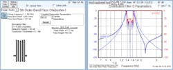
Figure 1 shows the top portion of the FD2D user interface. The example presented here is a microstrip interdigital bandpass filter with a center frequency of 1.5 GHz. FD2D allows users to select several Shape Types. Here, Chebyshev I is selected. In addition, the Pass Band Width is specified to be 250 MHz, while the Stop Band Width is set to 700 MHz. Furthermore, the substrate for this filter is 30-mil-thick alumina. The rest of the parameters can be seen in Figure 1. It should be noted that the Enable Extensions checkbox is checked to enable resonator length extensions for optimization.
1. Shown is the FD2D interface with the entered parameters.
Figure 2 reveals the bottom portion of the FD2D user interface, with the S-parameters of the filter shown on the right. The thin traces represent an ideal response, while the darker traces depict more realistic S-parameters that account for parasitic effects.
2. S-parameters are generated in FD2D based on the parameters specified.
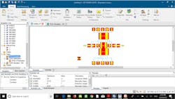
Now, the filter can be exported to CST Studio Suite in just seconds by clicking the CST Design Studio icon, shown at the top left corner of Figure 2. Figure 3 reveals the generated filter schematic in CST Studio Suite. As shown, the filter consists of various blocks that represent the microstrip interdigital filter elements.
3. After exporting the filter from FD2D, a filter schematic is generated in CST Studio Suite.
A circuit analysis can be executed by right-clicking FD2D Simulation in the navigation tree and then clicking Update. Figure 4 shows the resulting S-parameter plots, which are clearly unsatisfactory. Hence, optimization is required.
4. These are the S-parameter plots from the initial schematic simulation.
An Introduction to FD3D
Before continuing, it’s helpful to first explain FD3D in some detail. As mentioned, FD3D features what’s known as coupling matrix extraction, which involves importing the S-parameters of a filter. Once the S-parameters are imported, a coupling matrix can be quickly extracted for that specific response.
When utilizing coupling matrix extraction for filter optimization, the extracted coupling matrix is compared to a synthesized coupling matrix. This synthesized coupling matrix corresponds to the desired filter performance. By comparing the extracted coupling matrix with the ideal synthesized one, problematic areas in the model can be identified. In turn, the model dimensions are changed accordingly. This cycle is repeated until the filter is tuned to a state in which it achieves an acceptable level of performance.
Coupling matrix extraction offers several benefits. For one, an optimization based on coupling matrices can execute in less time than a standard optimization based on S-parameters. In addition, it can help designers locate problematic or parasitic couplings. Thanks to coupling matrix extraction, designers are able to tune the relevant parameters of the filter geometry.
Optimizing the Filter Schematic
Continuing with the example, the filter can now be optimized with the help of FD3D. First, to open FD3D, click Filter Synthesis in the ribbon bar when in the schematic view and then select Filter Designer 3D. Upon opening FD3D, users can enter the passband specifications, which determine the optimization goals. For the passband specifications in this example, Order is set to 5, Return Loss is set to 25, Start (frequency in GHz) is set to 1.375, and Stop (frequency in GHz) is set to 1.625 (Fig. 5).
5. FD3D allows users to define the passband specifications for a bandpass filter.
FD3D also gives users the option to specify transmission zeros. However, no transmission zeros will be added in this case, since an inline filter is being designed (a transmission zero is present, but that’s due to the uncontrollable cross-coupling in the interdigital layout).
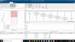
Clicking the Matrix tab reveals the different topologies that can be employed to realize the specified filter (Fig. 6). Here, a fifth-order mainline coupling topology is selected. Figure 6 also displays the coupling matrix that’s automatically synthesized based on the specifications and topology.
6. With FD3D, designers are able to select different topologies that can be implemented to achieve the specified performance.
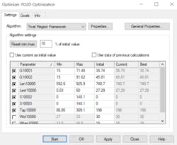
Before closing FD3D, save the FD3D file. After returning to CST Studio Suite, the goal is to now optimize the filter. Double-clicking FD2D Optimization in the navigation tree prompts users to specify the optimization settings and goals (Fig. 7). To obtain the desired performance, the selected parameters shown in Figure 7 will be tuned. These parameters include G10001 and G10002, which denote the resonator separations. Len10000 represents the conductor lengths, while Lext10000 denotes the end extensions. S10002 and S10003 indicate the extension lengths, and Tap10000 represents the tap position.
7. The optimization settings reveal the parameters that will be tuned to meet the design goals.
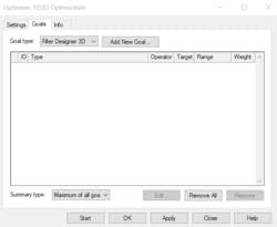
The optimization goals can be specified by clicking the Goals tab (Fig. 8). After selecting Remove All to delete all pre-defined goals, Filter Designer 3D is then selected as the Goal type. By making this selection, it will execute an FD3D-based optimization rather than a standard version. Clicking Add New Goal automatically opens FD3D once again.
8. FD3D must be specified when setting the optimization goals.
Once FD3D is open, the previously saved FD3D file can be imported by selecting File>Import. It’s important to now specify the matrix-extraction settings in FD3D, which can be accomplished by clicking the Matrix tab and then selecting Matrix Extraction. Figure 9 shows the settings used in this example. Checking the Limit Extraction Range checkbox limits the frequency range and the amplitude for the samples utilized for extraction. The Parasitic Extraction checkbox is also selected so that the software can take into account parasitic transmission effects like the unintended cross-couplings that cause the high-side transmission zero in this interdigital configuration.
9. The settings for the matrix extraction include the start and stop frequency and more.
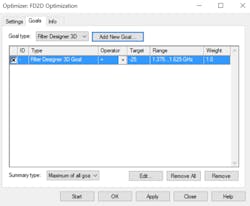
The next step is to apply FD3D to the project by clicking File>Apply. Closing FD3D and returning to CST Studio Suite reveals that the parameters from FD3D have been applied to the optimization goals (Fig. 10). Clicking Start will begin the optimization.
10. The specifications defined in FD3D are now applied to the optimization goals.
After the optimization is complete, the new S-parameter plots of the filter can be viewed by clicking S-Parameters under FD2D Optimization in the navigation tree (Fig. 11). Since the new S-parameters reveal dramatically improved performance, the first step of the design process is now complete.
11. The S-parameter plots from the optimized schematic simulation reveal a significant improvement.
Simulation of the 3D Model
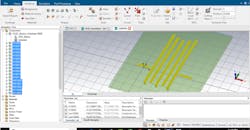
The filter schematic has been optimized to achieve acceptable S-parameter simulation results. Now it’s time to begin the second step of the design process: Perform an EM analysis of the 3D model of the filter. Since the filter schematic has been optimized, a 3D model based on the schematic should be a good starting point for the EM analysis.
One additional step is required before simulating the 3D model. It’s necessary to merge all metallic microstrip filter elements on the top layer, as the filter is automatically generated with various microstrip components that are joined together. Merging these metallic elements will remove unnecessary faces in the model that are undesirable for the meshing.
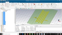
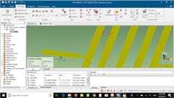
Merging the metallic elements can be carried out by selecting all of the microstrip components, which are found under Components in the navigation tree (Fig. 12). Next, by clicking Boolean in the ribbon bar and then selecting Add, the components are able to be merged.
12. Merging the metallic filter elements is a necessary step in this example.
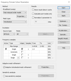
The 3D model can now be simulated. Selecting Setup Solver from the ribbon bar reveals the frequency-domain solver parameters. Figure 13 shows the settings implemented in this example. Clicking Start begins the simulation.
13. The frequency-domain solver parameters include the frequency settings and more.
Figure 14 illustrates the resulting S-parameter plots of the 3D EM simulation. The filter clearly does not achieve the desired goals—the performance at the high end of the specified passband is not acceptable. Therefore, optimization is required once again.
14. The S-parameter results from the initial EM simulation demonstrate that the filter does not meet the performance goals. Denoted are all four S-parameter values at 1.625 GHz.
The Final Step: Optimizing the 3D Model
At this stage, “face constraint parameters” will be added before optimizing the 3D model. While such parameters are not required for optimization, using them makes it possible to calculate sensitivities that speed up the simulation. The different face constraint parameters, which will serve as the tunable filter parameters, correspond to the resonator lengths and the amount of separation between resonators.
To create the face constraint parameters that will define the tunable resonator lengths in this example, follow these steps:
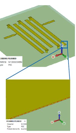
- Select Picks from the ribbon bar followed by Pick Face (or simply hit the ‘f’ the shortcut key). Next, click the end face of the open-ended side of the first resonator (Fig. 15).
- Click the Local Modification dropdown in the ribbon bar followed by Define Face Constraints.
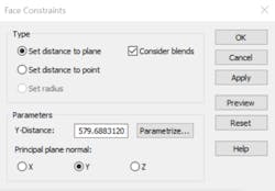
- Select Y as the Principal plane normal (Fig. 16). In addition, clicking Parametrize allows users to enter a parameter name.
- Repeat steps 1 to 3 for all other resonators.
15. In this example, creating a face constraint parameter to define a tunable resonator length began by selecting the end face of the resonator’s open-ended side.
16. When defining face constraints, users can specify whether the distance should be set with respect to a plane or a point.
Once the face constraint parameters that correspond to all of the resonator lengths are defined, the next step is to create the face constraint parameters that will define the tunable amount of separation between resonators. This can be accomplished with the following steps:
- Select the Pick Points dropdown followed by Pick Edge Center (or simply hit the ‘m’ shortcut key) to select the top edge of the first resonator that’s adjacent to the second resonator. Use the Pick Edge Center function again to select the top edge of the second resonator that’s adjacent to the first resonator (Fig. 17).
- Next, select Mean Last Two Points (also located under the Pick Points dropdown), which will result in the creation of a single point located between the two resonators.
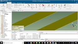
- Use the Pick Face function (‘f’ shortcut key) to select the inside face of the first resonator that’s facing the point (Fig. 18).
- Click the Local Modification dropdown in the ribbon bar followed by Define Face Constraints.
- Select Set distance to point (Fig. 16, again). Click Parametrize to enter a name for the parameter.
- Next, repeat steps 1 and 2 and then use the Pick Face function (‘f’ shortcut key) to select the inside face of the second resonator that’s facing the point.
- Repeat steps 4 and 5.
17. In this case, creating face constraint parameters to define an area of separation between resonators began by placing a point on the top edge of both adjacent resonators.
18. Here, the inside face of one resonator is selected. A face constraint parameter will be defined with respect to the point shown to ultimately define the tunable amount of separation between both resonators pictured.
These seven steps should be repeated to create the face constraint parameters for the remaining areas of separation between resonators. Furthermore, clicking the Local Modification dropdown followed by Show Face Constraints allows users to view all the face constraint parameters.
Now that all face constraint parameters have been defined, the optimization process can begin. After selecting Setup Solver from the ribbon bar, check the Use sensitivity analysis checkbox to allow for a more efficient optimization (Fig. 13, again). Selecting this option will activate the corresponding Properties button, which can be clicked to ensure that all created face constraint parameters are selected for the sensitivity analysis.
Now, to configure the optimization in a similar manner as before, click the Optimizer button (also found in the ribbon bar). The main difference here is that the newly created face constraint parameters must be selected for optimization rather than the parameters used previously to optimize the filter schematic. In addition, the Properties button can be selected to specify the Max. number of evaluations, Domain accuracy, and Finite difference. These parameters are set to 80, 0.01, and 0.01, respectively. In addition, clicking the General Properties button allows users to activate the move mesh feature for the optimization process, enabling a faster convergence. When optimizing narrowband filters, the move mesh feature plays an important role in terms of achieving convergence.
The same process of defining the optimization goals can be carried out by clicking the Goals tab (Fig. 8, again). With Filter Designer 3D again selected as the Goal type, one can select Remove All to delete all pre-defined goals and then click Add New Goal to automatically open FD3D once more.
The same process of importing the previously created FD3D file must be performed. Figure 19 shows the matrix-extraction settings that will be used this time. In addition to the Parasitic Extraction checkbox, both Lossy Extraction and Adapt Return Loss are selected. When Lossy Extraction is enabled, the software takes into account loss when performing the extraction.
19. These are the matrix extraction settings used for the EM optimization.
Activating the Adapt Return Loss function allows the software to adapt the return loss of the synthesized comparison matrix so that it matches the extracted return loss. This feature should be used when the input/output couplings are not controllable. In this case, since face constraint parameters were not created to correspond to the input/output feed-line positions, these positions cannot be controlled. Alternatively, face constraint parameters could have been created to correspond to the input/output feed-line positions.
After selecting File>Apply and closing FD3D, return to CST Studio Suite—it shows that FD3D has been applied to the optimization goals. Clicking Start will begin the optimization.
Figure 20 shows the S-parameter results of the optimized 3D model. The results reveal that S11 is below −25 dB throughout the entire passband. The design process is now complete. Furthermore, the optimization required 23 solver runs to achieve the goal function value.
20. The simulated S-parameter results of the optimized 3D model reveal that the filter meets the performance goals.
In summary, the software tools from Dassault Systèmes are a unique approach to filter design that can benefit all filter designers. This article presented one specific example, a microstrip interdigital filter. However, the tools utilized to design this filter will work with many other types, including cavity and dielectric filters. Anyone tasked with this responsibility may want to check out these tools.
