What you’ll learn:
- A compact 8-bit, 8-GS/s, time-interleaved SAR-based ADC will serve as a basis for next-generation, high-speed, broadband radios.
- The development of a 140-GHz front-end module shows how silicon technology can be leveraged to build competitive phased arrays for short-range, beyond-5G applications.
- Further research will explore how III-V materials can be teamed with CMOS technology to create efficient and cost-effective mobile device technology at 100 GHz and beyond.
Over the past two decades, advances in the telecommunications industry have largely been driven by the rapidly growing bandwidth requirements of online applications. Not only have the actual services become increasingly data-intensive (think of video streaming or over-the-air automotive software updates), but our digital and multiscreen lifestyles have also fueled this bandwidth explosion.
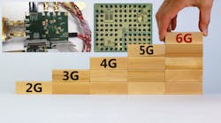
Successive generations of fixed and mobile network technologies have been developed and deployed to meet the demand for greater throughput. Mobile networks, specifically, focused on using higher radio frequencies, as higher frequencies equal more bandwidth. Case in point: 3G networks operate primarily in the 900-MHz and 2.1-GHz bands, while 4G networks are limited to frequencies of up to 2.5 GHz. 5G networks are pushing into the 28- and 39-GHz bands. Still, our hunger for bandwidth remains insatiable.
Discussion is ongoing about the exact characteristics and performance specs of next-generation (beyond 5G) wireless networks. What’s clear, though, is that they will largely outsmart their predecessors. Projected features include a 100-Gb/s single-link throughput, microsecond latency, and a significantly higher energy efficiency of less than 1 nanojoule per bit.
All of those features will be crucial to enable concepts such as federated learning between artificial-intelligence-enabled (AI) autonomous systems (such as self-driving cars), the deployment of very high-speed and ultra-reliable mobile hot spots in dense urban centers, or the support of immersive augmented-reality (AR) applications and holography.
To do so, ensuing generations of mobile networks (including 6G) will most likely look to frequencies above 100 GHz. Yet, as frequencies increase, mobile networks’ underlying (chip) technologies realize their limits, lacking the required transmit power and energy efficiency to operate at those frequencies in a cost-effective manner. This article provides an update on how this issue can be solved, presenting two recent research outcomes that demonstrate the viability of high-frequency (>100 GHz) wideband wireless communication for next-generation mobile devices.
Analog-to-Digital Converter Advances
High-speed analog-to-digital converters (ADCs) with a 7- to 8-bit resolution are a key component of the radio equipment embedded in next-generation broadband communication devices. Unfortunately, ADC power consumption dramatically increases as we tap into higher frequencies. This will likely become a major issue for battery-powered (6G) smartphones.
Using time-interleaved (TI), successive-approximation-register (SAR) ADCs has been an important first step to making ADCs more power-efficient. On the downside, though, they suffer from limited speed due to their underlying sequential conversion mechanism.
Consequently, imec researchers implemented speed-enhancing techniques in a compact single-bit, single-comparator SAR loop. Their design translates into an impressive 1 GS/s per channel, with a limited signal-to-noise distortion ratio (SNDR) degradation.
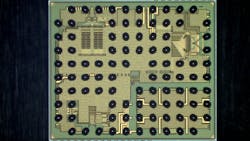
imec's 8-bit, 8-GS/s TI SAR ADC, which is fabricated in a 16-nm CMOS process and with an active area of 210 × 110 µm², consumes a mere 26 mW (Fig. 1). That’s significantly lower than the energy consumption reported by competitive TI SAR approaches. Moreover, the device achieves a 45-dB SNDR with 1-GS/s channels. We hope this contribution will be instrumental in developing the next wave of high-speed broadband radio transceivers that come with acceptable power-consumption levels.
Improvements to T/R Front-End Modules
The first radio band identified to accommodate beyond-5G services is the D-band, which ranges between 110 and 170 GHz. However, using standard silicon (CMOS-based) technologies at those frequencies isn’t an obvious choice, given that CMOS yields limited transmit power and power efficiency.
Yet, imec’s 140-GHz front-end module (FEM), fabricated in 22-nm FD-SOI CMOS, shows how silicon technology can still be leveraged to build competitive phased arrays for short-range beyond-5G applications. Thanks to its integrated switch functionality, the same antenna array can be used for the transmit and receive (T/R) modes in a time-division-duplex (TDD) communication system.
Integrating such a T/R in advanced silicon technology typically comes with significant losses in output power and efficiency. However, by introducing a new topology that avoids using a dedicated switch in the transmit path, those losses are considerably reduced.
Concretely, this compact D-band FEM with integrated T/R switch functionality achieves a saturated output power (Psat) of 12.5 dBm, and a peak-power added efficiency of 11% in transmit mode. In receive mode, it achieves a 9.2-dB noise figure for the receiver with just 20-mW power consumption from a 0.8-V supply.
What’s Next: A Research Pipeline Filled to the Brim
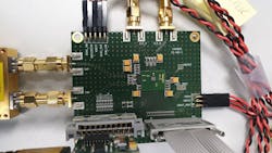
By the end of 2022, these components will be integrated into a new RF module for telecom vendors to experiment with (Fig. 2). And there’s yet more to come, as imec researchers have begun exploring a hybrid III-V/CMOS approach to enable medium- to long-range applications at frequencies over 100 GHz.
The aim is to substantially reduce the footprint and power consumption of next-generation radios. The problem is that III/V materials, such as indium phosphide (InP), only come in small wafers, making them less suited for mass-market consumer applications. In addition, they typically have a limited back end of line (BEOL), which hampers the implementation of complex circuits. On top of that, they tend to come with a lower yield.
As part of imec’s Advanced RF program, we try to overcome these limitations. We’ll also continue investigation into how III-V materials can heterogeneously be combined with CMOS technology to create mobile device technology that efficiently and cost-effectively operates at 100 GHz and beyond.


