Tackling Terahertz Transceiver Design
This file type includes high resolution graphics and schematics.
Bandwidth demands are driving operating frequencies constantly higher, with submillimeter-wave and terahertz frequency bands offering tremendous potential for applications in indoor wireless communications, spectroscopy, and imaging systems. Frequencies between 275 and 3000 GHz, which have not yet been officially allocated, offer tremendous growth potential for near-field communications at data rates of 10 Gb/s and higher in the near future.1-4 The challenge facing design engineers is the development of affordable hardware to support applications operating at such high frequencies.
Terahertz imaging and spectroscopy, for example, are among the more interesting applications for medical and industrial applications of terahertz frequencies. Terahertz imaging can be extremely useful for aircraft guiding and landing systems in zero-visibility situations. Millimeter-wave imaging systems can provide two-dimensional images of a landing area.5 Terahertz-based near-field communications can enable transfer of large amounts of data to multiple users within buildings.
Related Articles
• Cross-Spectral Phase Noise Is Measured On Terahertz Source
• Architecture Cracks Terahertz Power Generation And Tuning
• Terahertz Imaging System Uses BWO As Source
During the 2008 Olympic Games, Fuji Television Center used a terahertz system to transmit video signals of a live high-definition (HD) program from a recording studio to the international broadcast center, about 1 km distant. This organization achieved a data rate of 10 Gb/s in recent terahertz transmissions.6 The use of terahertz frequencies has increased in recent years as the output power of transmitters and the sensitivity of receivers at those frequencies has increased.
Terahertz communications devices are based on both photonic and electronic technologies, and different design equations apply to each technology area. Classical equations govern the submillimeter-wave spectrum while quantum equations are generally used for frequencies above the terahertz region. To better understand how they fit for higher-frequency applications, both technologies will be examined and then compared under different circumstances.
Using photonic technology, basic transmit and receive operations are performed in the optical regime with the appropriate devices. The transmitter has the required components for signal generation, modulation, amplification, and optical-to-electrical conversion (Fig. 1). The first step involves optical signal generation and the last step is optical-to-electrical conversion prior to the antenna.
1. This block diagram shows a photonics-based approach for a terahertz transmitter.
Solid-state and vacuum-tube devices have been used for signal generation at lower frequencies within the terahertz region, while beam-wave tubes and optically pumped lasers (OPLs) have been used for higher-frequency terahertz applications. Beam-wave tubes include gyrotrons and free-electron lasers (FELs). These sources provide high output-power levels and are often used for plasma heating, high-power radar systems, and remote-sensing systems. Vacuum electronic devices—such as FELs, electron cyclotron lasers, and Cherenkov wave devices—produce output signals to 1 THz, with cyclotron tubes capable of terahertz signals at power levels to 1 kW. In FELs, the electron beams oscillate at high speeds to release photons via a strong magnetic field. These photons are then directed, by means of a reflector, through the electron beam for added gain. Solid-state lasers provide sources of high-frequency energy,8 as do OPLs.7
Optical modulators include devices that work by modulating signals provided by optical sources, such as absorptive and refractive modulators. In an absorptive modulator, modulation is based on the variation of the absorption coefficient due to the Fermi level or free-carrier concentration changes. In a refractive modulator, operation is based on refractive index variations.9 Decreasing the frequency of an optical signal following generation from an optical source and prior to modulation is another method for producing terahertz and millimeter-wave modulation4; this approach can be implemented in a number of different ways.10-12 In one simple approach, millimeter-wave and terahertz signals are generated by means of a subharmonic mode-locked laser diode and an arrayed waveguide grating (AWG) filter (see Fig. 2).10 AWGs are commonly used as optical demultipliexers in wavelength-division-multiplex (WDM) systems.
2. This block diagram shows an electronics-based approach for a terahertz transmitter.
This file type includes high resolution graphics and schematics.
Additional Optical Amplifier Uses
This file type includes high resolution graphics and schematics.
Optical amplifiers are also key components used for processing optical and terahertz signals. Amplifiers are realized with a number of different technologies, including as laser, semiconductor optical, Raman, and optical parametric amplifiers. Two major categories of optical amplifiers include fiber-based and planar optical waveguide amplifiers.13
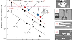
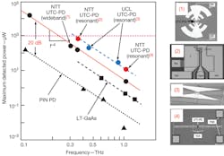
For photonic based transmitters, optical-electric (O/E) converters are key devices. Unitraveling-carrier photodiodes (UTC-PDs) and photodiodedevices based on positive-intrinsic-negative (PIN) photodiodes (PIN PDs) serve as efficient O/E converters. A combination of these two approaches can provide conversion with reasonable output power through 380 GHz, with photocurrent of 10 mA and bias voltage of 1.1 V yielding output power of 110 μW. This output power can be increased to 400 μW using photocurrent of 20 mA. Figure 3 depicts output powers for three O/E converter technologies: UTC-PD, PIN-PD, and low-temperature (LT) GaAs photomixers.2
3. This plot compares the high-frequency performance of three O/E converter technologies: UTC-PD, PIN-PD and low-temperature (LT) GaAs photomixers.
As the use of different electronic devices has shown over the past few years, the performance of terahertz systems can be steadily improved, including the noise and phase performance. Figure 4 shows the conceptual design of a transceiver for terahertz applications, to demonstrate how different electronic devices, such as sources, modulators, transistors, and amplifiers, can be applied to improve the performance of terahertz transceiver systems.
4. This simple block diagram shows an electronic terrhertz transceiver.
A variety of electronic sources for terahertz applications have been developed in recent years. Some of the signal sources are integrated-circuit (IC) oscillators based on transistors, resonant tunable diodes,14 Bloch oscillators,15 or plasmaticoscillators.16 Hot-electron-bolometer (HEB) superconductor mixers have also been developed over the past decade, providing some of the highest sensitivity levels for heterodyne receivers at frequencies above 1 THz. Low-noise amplifiers (LNAs) based on indium-phosphide (InP) high-electron-mobility-transistor (HEMT) devices are also capable of operation at these frequencies.17
At the conjunction of these two technologies, fourth or quad pixel technology limits noise levels for high-speed spectroscopy and imaging applications. The operation and processing speed of these pixel-based systems can be significantly improved by means of integrated HEB circuits and intermediate-frequency (IF) amplifiers integrated in multipixel focal plane arrays (FPAs).18 The low power consumption of LO sources and the low operational noise of HEB mixers make them suitable for this kind of integration, especially in monolithic-microwave-integrated-circuit (MMIC) IF amplifiers. Proper use of input matching networks provides the necessary frequency tuning and opportunities for using MMIC devices with different sources and at different operating frequencies. Chip devices based on single-pixel HEB array technology have been fabricated with close to 30-dB gain across bandwidths as wide as 10 GHz at terahertz frequencies.
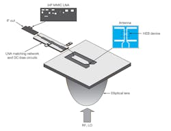
Figure 5 shows the base structure of a single-pixel HEB array.17 The active elements consist of a photon-cooled HEB, constructed from NbN films deposited on a silicon substrate. The three composite focal plane elements, which consist of HEB and MMIC IF amplifiers, have demonstrated operation at frequencies to 1.6 THz. In theory, the integrated quasioptical pixels can be operated at even higher frequencies. Research has indicated the possibility for developing FPAs with potentially hundreds of pixels. High-frequency HEB FPAs can be useful in applications such as astronomy, long-distance detection, and medical diagnostic systems.
5. These are the essential components of a single-pixel HEB.
This file type includes high resolution graphics and schematics.
Further Research Trends
This file type includes high resolution graphics and schematics.
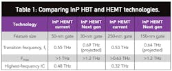
While these exotic devices offer great promise at higher frequencies, one of the most important devices for terahertz systems is still the common transistor, which is used throughout high-frequency systems. A number of researchers have focused on extending the frequency range of commonly used devices, such as InP HEMTs and HBTs.19 InP HEMTs with maximum frequencies between 0.5 and 0.65 THz and HBTs with frequencies from 0.3 to 0.4 THz have already been reported.20 Considering the results of these reports, and the research being conducted by DARPA, the upper frequency limits of these devices should only increase. Table 1 provides a summary of various research being performed on these two types of high-frequency transistors.21 Recently, a research team presented a new InP HEMT device with average frequency of 0.55 THz and maximum frequency of more than 1 THz.
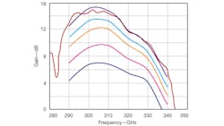
To develop higher-frequency transistors for possible terahertz use, a number of studies have explored the use of 100-kV electron beam lithography (EBL) to fabricate devices with the fine dimensions needed for higher-frequency operation.21 In one report, researchers have fabricated an HBT device with emitter width of 0.15 μm. In addition, an advanced InP HEMT was fabricated with emitter area of 0.25 × 4 μm2 and breakdown voltage of 4 V with maximum current gain of 30. The measured S-parameters for this transistor indicate a maximum frequency of operation of more than 650 GHz.Some InP HEMT and metamorphic HEMT (mHEMT) transistors with operating frequencies between 300 and 350 GHz have also been introduced.22 Based on these researches and technologies, an amplifier with gain of more than 11 dB and frequency of 480 GHz was proposed. Figure 6 shows the gain versus frequency for a 300-GHz amplifier. For a three-stage amplifier based on this amplifier, maximum gain of 15 dB at 15 THz was achieved. However, the three-stage amplifier suffers non ideal noise characteristics at its input amplifier stage.21
6. The gain of a 300-GHz amplifier is plotted across an approximate 50-GHz bandwidth.
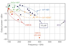
Figure 7 summarizes recent activity on oscillator ICs operating at 100 to 600 GHz. All of these devices offer output power of more than 10 μW, considered a minimum power level for practical operation. The core research in this area focuses on transistors and MMICs, with HBT transistors having cutoff frequencies to 0.8 THz and HEMT transistors with frequencies to 1 THz already having been reported.23 The characteristics of InP-based devices indicates that they are more suitable for terahertz applications than silicon-based devices, although devices based on silicon-germanium (SiGe) substrates are showing great promise at higher frequencies.
7. These plots compare the output levels of IC oscillators based on different semiconductor technologies.
The challenges for producing terahertz transistors include decreasing device dimensions while also overcoming the effects of parasitic circuit/device elements at higher frequencies. For HBTs, small emitter dimensions are needed with low contact resistance between the base and emitter as well as reduced capacitance between the base and collector. Experimental HBTs have been developed to 500 GHz, compared to silicon circuits which reached a maximum of 96 GHz. In addition, an InP HEMT with breakdown voltage of 2.5 V and current of 0.25 mA/mm for an operating frequency of 1.2 THz has been proposed. A number of studies have focused on exploring the performance capabilities of InP HBT devices.24 One of the main challenges is balancing the current increase that occurs when the InP HBT device dimensions are reduced, and the need to dissipate the added heat generated by additional current flow. One possible solution involves changing the connection width and reversing the power, thus increasing the heat resistance capability. Practical terahertz bandwidths can only be achieved with these devices when the ohmic contact resistance is very low.
A proposed terahertz-frequency modulator is based on a HEMT device in which a two-dimensional electron gas (2DEG) is used as the interface layer for the GaAs/AlGaAs substrate material. The electron density of the 2DEG can be tuned and controlled by the external gate voltage. Experiments performed on this structure used an applied voltage between 0 and 10 V. The cutoff frequency based on the growth of received signal was calculated as 6 kHz. With an applied gate voltage of 10 V, a maximum modulated terahertz wave of 3% was obtained using terahertz time-domain spectroscopy (TDS). By creating forms of artificial metals known as metamaterials, it has been possible to create split ring resonators (SRRs) with extremely high frequencies.25 The metamaterials have been analyzed by means of Maxwell’s equations for different properties—such as electron permittivity and magnetic permeability—and these materials show great promise for use at terahertz frequencies.
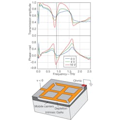
8. These plots show the amplitude (top) and phase (middle) performance of a terahertz electronic modulator (bottom).
This file type includes high resolution graphics and schematics.
Conclusions
This file type includes high resolution graphics and schematics.
Since these materials can be influenced by an external applied voltage, the metamaterial resonance can be switched from active and passive and back again by tuning the sublayer conductivity.25 A hybrid semiconductor formed of these materials consists of SRR electronic plates fabricated on a 1-μm Si-GaAs layer [Fig. 8(a)]. By connecting all SRRs, the structure resembles a Schottky gate in function.25 The carrier electron density can be completely controlled by a reverse voltage, making control of metamaterial resonance and terahertz operation possible [Fig. 8(b)]. This structure can operate with 50% modulation depth at less than 15 V applied bias voltage.26 These metamaterial modulators offer potential as high-speed modulators for imaging and communications applications.27
A spatial light modulator (SLM), which can operate in the terahertz region, is capable of electronic and optical control of transmission and reflection of an optical beam and as a result change of direction and advance coding. These devices are essential for many optical and electronic applications, including imaging and spectroscopy.28 By introducing this technology for use in the terahertz region, it can play an important role in spectroscopy and communication applications.29 As an example, in recent terahertz single pixel imaging, an SLM served as a key component for decoding to terahertz waves.29
9. This schematic diagram shows the components in an amplifier designed for use from 160 to 180 GHz.
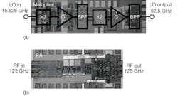
Figure 9 shows an amplifier consisting of five 150-GHz stages designed to operate between 160 and 180 GHz. It includes three cascaded stages and two common emitters. The final stage consists of two devices in parallel to achieve high output power. The amplifier is optimized by tuning its resistors, capacitors, and inductors for operation between 140 and 170 GHz. For operation at 170 GHz, capacitors with values of less than 30 fF are required. For such small capacitance values, a metal-oxide-metal structure was developed. Figure 10 offers a MMIC multiplier and amplifier for terahertz use; the MMIC amplifier consists of five simple stages.
10. These photographs offer a multiplier (a) and amplifier (b) designed to produce 125-GHz output signals.
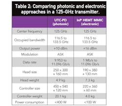
Both photonic and electronic means are capable of reaching terahertz frequencies. As a comparison, Table 2 shows specifications for a 125-GHz transmitter realized by means of photonic (UTC-PD) and electronic (InP HEMT MMIC) approaches.2,4 Each method has advantages and disadvantages, with electronic approaches being somewhat limited in usable output-power levels and photonic approaches also allowing fiber connections from point to point in a system. The technologies are steadily improving, making terahertz applications more feasible in the near future.
A. Mohammadi, Researcher
Faculty of Electrical Engineering, Amirkabir University of Technology (Tehran Polytechnic), Tehran, Iran; e-mail: [email protected].
M. Danaeifar, Researcher
Faculty of Electrical and Computer Engineering, K.N. Toosi University of Technology, Tehran, Iran.
References
1. Ho-Jin Song and Tadao Nagatsuma, “Present and Future of Terahertz Communications,” IEEE Transactions On Terahertz Science And Technology, Vol. 1, 2011, p. 1.
2. T. Kleine-Ostmann and T. Nagatsuma, “A review on terahertz communications research,” Journal on Infrared, Millimeter, and Terahertz Waves, Vol. 32, 2011, p. 143.
3. J. Federici and L. Moeller, “Review of terahertz and subterahertz wireless communications,” Journal of Applied Physics Vol. 107, 2010, p. 111.
Related Articles
• Cross-Spectral Phase Noise Is Measured On Terahertz Source
• Architecture Cracks Terahertz Power Generation And Tuning
• Terahertz Imaging System Uses BWO As Source
4. Jin-Wei Shi, Chen-Bin Huang, and Ci-Ling Pan, “Millimeter-wave photonic wireless links for very high data rate communication,” NPG Asia Mater Vol. 3, 2011, p. 41.
5. Mustafa Rangwala, Feinian Wang, and Kamal Sarabandi, “Study of Millimeter-Wave Radar for Helicopter Assisted-Land ing System,” IEEE Antennas and Propagation Magazine, Vol. 50, 2008, p. 2.
6. Akihiko Hirata, Toshihiko Kosugi, Hiroyuki Takahashi, et al., “120-GHz-Band Wireless Link Technologies for Outdoor 10-Gbit/s Data Transmission,” IEEE Transactions On Microwave Theory & Techniques, Vol. 60, 2012, p. 3.
7. G.F. Brand, “Development and Applications of Frequency Tunable, Submillimeter-Wave Gyrotrons,” International Journal of Infrared and Millimeter Waves, Vol. 16,1995, p. 879.
8. X. Yin, “Terahertz Imaging for Biomedical Applications: Pattern Recognition and Tomographic Reconstruction,” Vol. 10, 2012, p. 1007.
9. Chen-Bin Huang, Sang-Gyu Park, Daniel E. Leaird, and Andrew M. Weiner, “Nonlinearly broadened phase-modulated continuous-wave laser frequency combs characterized using DPSK decoding,” Vol. 16, 2008, p. 2520.
10. Akihiko Hirata, Mitsuru Harada, and Tadao Nagatsuma, “120-GHz Wireless Link Using Photonic Techniques for Generation, Modulation, and Emission of Millimeter-Wave Signals,” Journal of Lightwave Technology, Vol. 21, 2003, p. 2145.
11. Zhensheng Jia, G.A. Jianjun Yu, Yu-Ting Hsueh, A. Chowdhury, et al., “Multiband Signal Generation and Dispersion-Tolerant Transmission Based on Photonic Frequency Tripling Technology for 60-GHz Radio-Over-Fiber Systems,” IEEE Photonics Technology, Vol. 20, 2008, p. 1027.
12. F.-M.Kuo, J.-W. Shi, H.-C. Chiang, H.-P. Chuang, et al., “Spectral Power Enhancement in a 100 GHz Photonic Millimeter-Wave Generator Enabled by Spectral Line-by-Line Pulse Shaping,” IEEE Photonics Journal, Vol. 2, 2010, p. 719.
13. John D. Albrecht, Mark J. Rosker, H. Bruce Wallacet, and Tsu-Hsi Chang, “THz Electronics Projects at DARPA: Transistors, TMICs, and Amplifiers,” IEEE MTT-S International, Vol. 978, 2010, p. 1118.
14. M. Asada, N. Orihashi, and S. Suzuki, “Voltage-controlled harmonic oscillation at about 1 THz in resonant tunneling diodes integrated with slot antennas,” Japanese Journal of Applied Physics, Vol. 46, 2007, p. 2904.
15. T. Unuma, N. Sekine, and K. Hirakawa, “Dephasing of Bloch oscillating electrons in GaAs-based superlattices due to interface roughness scattering,” Applied Physics Letters, Vol. 89, 2006, p. 161913.
16. T. Suemitsu, Y.M. Meziani, Y. Hosono, M. Hanabe, T. Otsuji, and E. Sano, “Novel plasmon-resonant terahertz-wave emitter using a double-decked HEMT structure,” DRC (Tohoku University, Sendai, 18-20 June 2007), p. 157.
17. W.R. Deal, “Solid-State Amplifiers for Terahertz Electronics Northrop Grumman Aerospace Systems,” IEEE MTT-S International (Redondo Beach CA, May 23-28, 2010), p. 90278.
18. B. Chan, B. Oyama, C. Monier, and A. Gutierrez-Aitken, “An ultra-wideband 7-bit 5-Gsps ADC implemented in submicron InP HBT technology,” IEEE Journal of Solid-State Circuits, Vol. 43, 2008, p. 2187.
19. V. Radisic, X.B. Mei, W.R. Deal, et al., “Demonstration of Sub-Millimeter Wave Fundamental Oscillators Using 35-nm InP HEMT Technology,” IEEE Microwave & Wireless Components Letters, Vol. 17, 2007, p. 223.
20. R. Lai, “Sub 50 nm InP HEMT Device with Fmax Greater than I THz,” IEEE IEDM Digest (Northrop Grumman Space Technology, Redondo Beach, CA, December 10-12, 2007), p. 609.
21. W. Snodgrass, “Pseudomorphic InP/lnGaAsheterojunction bipolar transistors (PHBTs) experimentally demonstrating ft = 765 GHz at 25°C increasing to ft = 845 GHz at -55°C,” IEEE International Electron Devices Meeting (SanFrancisco, CA, December 11-13, 2006).
22. Tong Chen, Willie J. Padilla, Joshua M.O. Zide et al., “Terahertz Switch/Modulator Based on Metamaterials,” IEEE, 2007.
23. Hou-Tong Chen, Willie J. Padilla, Michael J. Cich, et al., “A Broadband Terahertz Metamaterial Electrical Modulator,” IEEE, Vol. 978, 2009, p. 55752.
24. Wai Lam Chan, Hou-Tong Chen, Antoinette J. Taylor, et al., “A Spatial Light Modulator for Terahertz Radiation,” CLEQ/QELS Department of Electrical and Computer Engineering, Rice University (Houston, TX, June 2-4, 2009), p. 1.
25. D. Engstrom, J. Bengtsson, E. Eriksson, and M. Goksor, “A spatial light modulator for terahertz beams,” Optical Express, Vol. 16, 2008, p. 18275.
26. W. L. Chan, K. Charan, D. Takhar, et al., “A single-pixel terahertz imaging system based on compressed sensing,” Applied Physics Letters, Vol. 93, 2008, p. 121105.
27. C. Jastrow, K. Munter, R. Piesiewiczand, et al., “300 GHz transmission system,” Electronics Letters, Vol. 44, 2008, p. 213.
28. E. Laskin, K.W. Tang, K.H.K. Yau, et al., “170-GHz Transceiver with On-Chip Antennas in SiGe,” RFIC IEEE, Toronto University (Toronto, Canada, June 1, 2008), p. 637.
29. Toshihiko Kosugi, Masami Tokumitsu, Koichi Murata, et al., “120-GHz Tx/Rx Waveguide Modulesfor 1O-Gbit/s Wireless Link System,” CSIC IEEE, NTT Corp. (Atsugi, Japan, November 2006),p. 26.
This file type includes high resolution graphics and schematics.
