Integrated Front End Serves Satcom Receivers
This file type includes high resolution graphics and schematics when applicable.
Microwave front ends are a critical part of any high-frequency receiver architecture. They downconvert incoming signals from an antenna and pass along lower-frequency intermediate-frequency (IF) signals for further processing, typically to an analog-to-digital converter (ADC). By adopting a modular approach, an integrated front end was developed for satellite-communications (satcom) applications from 12.75 to 13.25 GHz. This front end is compact in size while also achieving outstanding electrical performance.
An effective front-end receiver design should provide good low-noise performance, as characterized by low receiver noise figure, and high gain at the frequencies of interest. For Ku-band sitcom applications, a receiver front end was designed for use from 12.75 to 13.25 GHz. This integrated front end consists of three independent function modules: a low-noise block downconverter (LNB) module, a local oscillator (LO) driver module, and a frequency downconversion module.
The LNB module includes a waveguide-to-microstrip transition, three stages of low-noise and high-gain amplifiers, and an image-reject filter. The LO driver module consists of an active frequency multiplier, a bandpass filter, and a driver amplifier. The frequency downconverter module incorporates a single-balanced frequency mixer (based on a low-barrier Schottky diode) and an intermediate-frequency (IF) bandpass filter to achieve the desired bandwidth and out-of-band rejection of unwanted signals. Active circuits in these modules are biased by means of a common sequential bias circuit.
The front end incorporates novel and compact filters to achieve small size and low insertion loss. The design of the front-end modules reduces the total parts count by using a single GaAs HEMT as the active device for all of the active circuits. The circuits are implemented using microwave-integrated-circuit (MIC) technology on alumina substrates. The modules are integrated into aluminium housings with a robust mechanical design to avoid undesired coupling and cavity oscillations. Figure 1 shows a block diagram of the different function blocks in the integrated front-end design.
Active Circuitry
The LNB module includes three amplifier stages (Fig. 2): a low-noise-amplifier (LNA) stage followed by two gain stages. These amplifier stages are conjugately matched and constructed with GaAs HEMT active devices. The operating frequency range of the LNA is 12.75 to 13.25 GHz. The devices are biased at 2.0 V dc and 15 mA. Since low noise figure is a critical parameter for the LNA, in-house-extracted S-parameters are used for the GaAs HEMT device (rather than supplied by the manufacturer), along with noise data for the device to determine the actual device phase response for Γopt for optimum impedance matching for low noise figure.
This is done since high-frequency package parasitic impedances may change the phase response of the device. By employing this design approach, it was possible to obtain a noise figure of 2.3 dB with gain of 26 dB for the LNB, with measured results closely matched to the computer simulated performance.
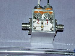
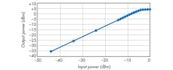
The design was simulated and developed by means of nonlinear analysis using harmonic-balance computer-aided-engineering (CAE) simulation software (Fig. 4). The GaAs HEMT active device in this doubler is operating in its pinchoff region to help achieve the aforementioned low conversion loss. This loss is 3 dB from C-band to Ku-band when operating with optimum input power of +2 dBm.
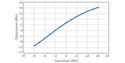
To achieve P1dB at low input power, the output load analysis of the driver amplifier was based on optimizing the small-signal gain, where the output load is maintained at a high value (based on load line analysis of the active device). This approach makes it possible to obtain higher gain compression at lower input signal level. The driver amplifier is biased at +2 V dc and 15 mA. It delivers 9-dB gain and provides +4.0 dBm output power (P1dB).
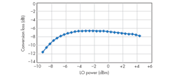
A single-balanced diode-based frequency mixer, which is part of the frequency downconversion module, was designed for operation from 12.2 to 13.2 GHz. The mixer incorporates low-barrier Schottky diodes operating at Ku-band frequencies at low LO drive levels. The mixer is designed with a 180-deg. hybrid for high RF-to-LO isolation and suppression of even-order harmonics generated by the LO.
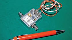
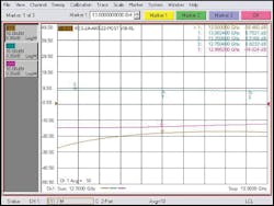
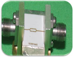
The image-reject filter, which is part of the amplifier module, was implemented as a resonator-type filter (Fig. 9). The function of the filter is to reject noise and signals at image frequencies. The filter, which measures 10 × 5 mm, has a bandwidth of 200 MHz with insertion loss of 2.5 dB, with better than 45-dB image rejection.
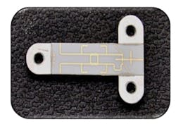
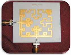
The IF filter, which is part of the frequency downconversion module, is based on microstrip transmission-line technology using a compact open-loop resonator.3-7 The filter is designed for a center frequency of 549 MHz and a bandwidth of 20 MHz with insertion loss of 4.0 dB across the passband. It provides maximum notch rejection of 40 dB and second-IF rejection of better than 25 dB.
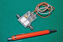
The filter measures 30 × 30 mm, which is compact for a component operating at UHF. Figure 10 shows a photograph of the fabricated IF filter. All three filters were designed with the aid of the LINMIC simulation software, now available from Computer Simulation Technology (CST). The circuit designs were verified using electromagnetic (EM) software simulation tools.
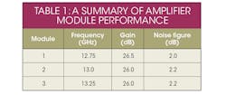
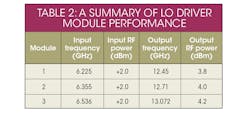
The three modules, along with an integrated bias card, were assembled into a front-end housing. The modules were characterized independently to determine performance levels prior to integration in the front-end housing. They were characterized over wide temperature extremes to ensure that minimum performance levels would be met even at operating temperature extremes. The various tables provide summaries of key performance parameters. Table 1 provides details on the amplifier module while Table 2 offers information on the performance of the LO driver module.
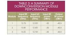
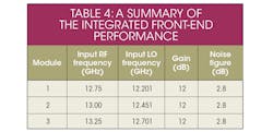
Table 3 presents details on the performance of the frequency downconversion module. It was characterized for a constant IF of 549 MHz and LO power of +4 dBm. Table 4 shows the performance attributes of the integrated microwave front-end assembly. The front-end subsystem is designed to operate with + 5 and -15 V dc supplies with DC power consumption of 0.7 W. The performance of the front-end system has been verified over an operating temperature range of -30 to +60°C. Variations in gain and noise figure as a function of temperature are controlled to better than ±1.0 and ±0.5 dB, respectively.
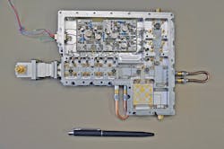
All three modules were integrated into a common modular package (Fig. 11). The circuits within these modules were implemented using MIC technology on alumina substrates, mounted on Kovar plates and interconnected by means of ribbon bond wires. The length and width of the ribbon bonds were optimized to less than 15 mils for an impedance match to 50 Ω.6 Tuning stubs near the ribbon bond wires were used to fine-tune any impedance mismatches in the interconnections.
Great care was taken in routing DC wire connections from the active stages (using short wire lengths to avoid radiating loops), such as the amplifier module and the LO driver module, to the integrated bias card to avoid undesired low-frequency oscillations. Ferrite beads were incorporated with feedthrough capacitors to form a lowpass filter, further rejecting spurious energy and avoiding in-band oscillations within the active circuits.
The housing was fabricated from 6061 aluminium alloy. It is designed to avoid mutual coupling between the gain stages and also avoid direct coupling between the LO drive module and the three-stage amplifier module. Cavity oscillations are minimized in these two modules by providing ground planes (conducting walls) and microwave absorbers at the electric field maxima regions. The modular front-end subsystem measures 150 × 180 × 20 mm and weighs 750 g. The compact front end was designed for integration into a command and ranging receiver for future spacecraft applications.
Acknowledgment
The authors would like to recognize the support and guidance from the senior colleagues of the Receiver Division of the Communication System Group (CSG) of the ISRO Satellite Centre (ISAC). Also, the authors are grateful for support provided to the Deputy Director of the ISRO Communication and Power area. The authors would also like to thank the Director of the ISRO Satellite Centre for encouragement during this work.
Avjit Roy Choudhury, Engineer
Deepankar Roy, Engineer
Alapati Venkata Sucharita, Engineer
Yateendra Mehta, Engineer
Communication System Group, ISRO Satellite Centre (ISAC), PB No. 1795 Vimanapura Post Bangalore - 560 017, Bangalore, India
R. Ramsubramanian, Engineer
Satellite Navigation Program, ISRO Satellite Centre (ISAC), PB No. 1795 Vimanapura Post Bangalore - 560 017, Bangalore, India
References
1. Jia-Sheng Hong and M. J. Lancaster, Microstrip Filters for RF/Microwave Applications, Wiley, New York, 2004.
2. Avjit Roy Choudhury and R. Ramsubramanian, “HEMT Modeling and
Validation for Low Power Nonlinear Circuits, 2013 ICMARS Proceedings.
3. Deepankar Roy, “Miniature Filter Screens VHF Band,” Microwaves & RF, July 2009.
4. Deepankar Roy and R. Ramasubramanian, “Planar Filter Provide High Image Rejection,” Microwaves and RF, October 2007.
5. LINMIC 6.2 +/N User Guide, Computer Simulation Technology.
6. Inder Bahl, Lumped Elements for RF and Microwave Circuits, Artech House, Norwood, MA.
7. Joseph S. Wong, “Microstrip Tapped-Line Filter Design,” IEEE Transactions on Microwave Theory & Techniques, Vol. MTT-27, No. 1, 1979, pp. 44-50.
This file type includes high resolution graphics and schematics when applicable.
