Download this article as a .PDF
Many systems require clean stable RF/microwave signals with programmable control. The LMX2594 phase-locked loop (PLL) frequency synthesizer from Texas Instruments provides the performance and flexibility from 10 MHz to 15 GHz that is as well suited to commercial communications as to military radar systems. It has an integrated voltage-controlled oscillator (VCO) and can generate output frequencies over that broad range with minimal spurious content and low phase noise.
The PLL has integer-N and 32-b fractional-N division modes with high phase-detector frequencies (400 MHz in integer-N mode and 300 MHz in fractional-N mode) that yield stable output signals with excellent spectral purity. The N-divider operates without a pre-divider to achieve the excellent spurious performance,
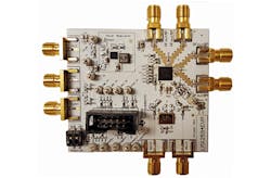
The LMX2594 (see photo) packs the VCO, programmable multipliers, dividers, multiplexers, and various control circuits into a 40-pin VQFN package that measures only 6.00 × 6.00 mm and runs on a single +3.3 V dc supply. It can operate with reference input signal frequencies from 5 to 1,400 MHz. The PLL’s integrated output driver amplifiers generate as much as +7 dBm output power at the highest frequencies. Output signals are clean, with single-sideband (SSB) phase noise of −110 dBc/Hz offset 100 kHz from a 15-GHz carrier. To meet critical synchronization requirements, the root-mean-square (RMS) jitter is a low 45 fs offset 100 Hz to 100 MHz from a 7.5-GHz carrier.
The on-board VCO is spectrally pure. Its one-octave frequency range of 7.5 to 15.0 GHz allows the frequency divider to handle frequencies below the lower bound but requires the use of frequency calibration to determine the correct VCO frequency band for a desired output frequency. Phase-noise measurements performed at frequencies within the different VCO bands, and at a supply voltage of +3.3 V dc and at room temperature (+25ºC), revealed low phase noise for all offsets and carrier frequencies.
For a carrier frequency of 8.0 GHz, the VCO’s phase noise is typically −80 dBc/Hz offset 10 kHz from the carrier, −107 dBc/Hz offset 100 kHz from the carrier, and −128 dBc/Hz offset 1 MHz from the carrier. For a 10.3-GHz carrier, the VCO’s phase noise is −77 dBc/Hz offset 10 kHz from the carrier, −104 dBc/Hz offset 100 kHz from the carrier, and −126 dBc/Hz offset 1 MHz from the carrier. For a 12.5-GHz carrier, the VCO phase noise is −74 dBc/Hz offset 10 kHz from the carrier, −100 dBc/Hz offset 100 kHz from the carrier, and −123 dBc/Hz offset 1 MHz from the carrier.
For applications that require multiple synchronized sources, such as phased-array radars and communications systems with multiple-input, multiple-output (MIMO) antenna arrays, the LMX2594 PLL provides the capability to synchronize the phase of output signals across multiple PLLs/synthesizers. A frequency ramp generator enables manual or automatic two-segment frequency ramp generation. In the manual mode, a user defines the rate of frequency range for the ramp. In the automatic mode, the ramp can be set up by means of two linear segments, with the PLL then establishing the slew rate for the ramp.
Changes in frequency are aided by a fast calibration algorithm that helps to accurately change frequencies in less than 20 μs while recalibrating the VCO as required in the middle of a waveform. The PLL’s on-board SYSREF controller makes the LMX2594 a strong candidate for a clock source for high-speed analog-to-digital converters (ADCs) and digital-to-analog converters (DACs). The PLL provides programmable delay adjustments in output signals to allow tuning as fine as 9 ps to account for signal delays caused by differences in coaxial cable lengths or transmission lines on PCBs.
The LMX2594 PLL combines a low-noise-signal-generating circuit configuration with a flexible and powerful control architecture to deliver a wide range of output waveforms across an impressively wide bandwidth. It can be driven with single-ended or differential input signals, and includes power-down modes to power the PLL up or down for energy conservation.
Texas Instruments, P.O. Box 655303, Dallas, TX 75265


