Refine Biasing Networks for High PA Low-Frequency Stability
Download this article in PDF format.
High-frequency active-device performance depends very much on the dc biasing conditions. For optimum performance, a solid-state device (SSD) requires an application-specific biasing network. Such bias networks are not only essential parts of RF/microwave circuits with SSDs, but properly designed bias networks contribute a great deal to the performance and stability of high-frequency circuits using SSDs.
SSD gain is inversely proportional to frequency, with higher gain at lower frequencies, so attention should be paid to SSD circuit design because of the strong connection between device gain and stability. For example, the response of an RF/microwave power amplifier (PA) should be carefully compensated to prevent oscillations due to the higher gain at lower frequencies.
At lower frequencies, the impact of the biasing networks is dominant compared to the impedance-matching networks. That’s because the small value of the dc blocking capacitor has a high impedance at lower frequencies, and neutralizes the effects of the matching networks. Thus, a properly designed biasing network can be employed to improve SSD low-frequency stability.
Although the stability analysis of RF/microwave circuits is a major topic, partial analysis allows for inferring some ideas about the low-frequency stability issues induced by biasing networks. The influences of PA biasing networks on low-frequency stability can be shown by analyzing the simplified low-frequency equivalent of a high-power field-effect transistor (FET) and its biasing networks.
Class AB type biasing will be considered for the low-frequency stability analysis. Following the analysis, design suggestions will be presented regarding gate and drain biasing, with attention paid to RF/microwave performance parameters such as insertion loss and efficiency. Finally, a resonance investigation study of a PA and its measured results will be presented.
Power-Amp ABCs
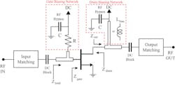
A typical PA consists of an active device and at least four passive subcircuits: input impedance matching, gate biasing, output impedance matching, and drain biasing. Figure 1 depicts such a structure. It is assumed that the values of the dc blocking capacitors are small enough to ignore the influence of matching networks on the analysis of the low-frequency response of the PA.
1. This is a conventional biasing structure for an RF/microwave power amplifier (PA).
To better understand the challenges of achieving low-frequency amplifier stability, the intrinsic transistor components and drain biasing structure will be used to show the initial conditions of low-frequency stability regarding input impedance and transfer function. The circuit complexity will be increased step by step to demonstrate the effects of the gate-biasing components.
The analysis steps are to determine the input impedance analysis without the gate-biasing components; include the serial bias resistor at the gate with an ideal RF bypass; and replace the ideal RF bypass capacitors with realistic capacitor models. This analysis will be performed for a narrowband high-frequency PA, with the term “low frequency” considered as applying to frequencies to a few hundred megahertz.
A conventional biasing structure of a PA includes a resistor at the gate and an inductor at the drain (Fig. 1, again). These components are RF shorted out at the dc supply point with a couple of RF bypass capacitors. Values of the dc blocking capacitors are often selected at picofarad level due to their low effective serial resistance (ESR) at the fundamental frequency and high self-resonance frequency (SRF). Therefore, the influence of matching networks can be neglected due to the high impedance of dc blocking capacitors in low frequency region.
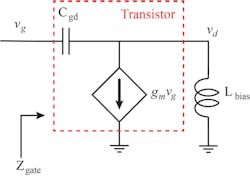
If an ideal RF bypass is assumed at the drain, then bias inductor Lbias has an ideal RF ground. The values of the intrinsic gate-source and drain-source capacitors, Cgs and Cds, respectively, are in the picofarad range so that they can be neglected as well at low frequencies. Capacitance Cgd is the intrinsic gate-drain capacitance of the transistor. Although Cgd is even smaller than Cgs and Cds, it is a feedback component of the circuit, so it has a significant role on stability.
2. Shown is a low-frequency equivalent circuit of an RF/microwave PA without biasing circuitry or biasing components.
With these assumptions, the low-frequency equivalent of a PA without gate-biasing network can be depicted (Fig. 2). Impedance Zgate is the impedance observed at the transistor gate:
Zgate = (ZCgd + ZLbias)/(1 + gmZLbias) (1)
Zgate(s)
= 1/sCgd + sLbias)/(1 + gmsLbias)
= (1 + s2LbiasCgd)/(sCdg + s2gmLbiasCgd) (2)
Zgate(jω)
= (1 – ω2LbiasCgd)/(jωCgd – ω2gmLbiasCgd) where s = jω (3)
Since ω is in the megahertz frequency range and the gate-drain capacitance Cgd is less than a few picofarads, ω2LbiasCgd << 1 and Eq. 4 holds:
Zgate(jω) = 1/(jωCgd – ω2gmLbiasCgd) (4)
and
Re{Zgate} ≈ 1/(ω2gmLbiasCgd) (5)
Oscillation startup conditions at a particular frequency can be described as1:
Re{Z, ω} < 0, Im{Z, ω} = 0 (6)
(∂Im{Z, ω})/∂ωǀω = ω0 ˃ 0 (7)
Eq. 5 shows that the real part of the impedance is negative at low frequencies. Although the negative resistance is not the only condition needed to cause oscillations (Eqs. 6 and 7), its elimination is a significant step in taking a PA into a safe zone against low-frequency oscillations. It is obvious that making the real part of impedance positive with the configuration of Fig. 2 is not possible.
Since gate-drain capacitance Cgd and transconductance gm are the intrinsic device parameters that depend on the transistor’s dc operating points, varying them affects circuit performance using that transistor. Therefore, a designer is only able to change the drain-biasing inductance value to decrease the negative resistance.
Yet, the drain-biasing inductance cannot simply be changed without consideration of other circuit parameters. For example, if the drain-biasing transmission line is a quarter-wavelength (λ/4) line, the low-frequency inductance of the line is given by2:
L = Z0(l/c) (8)
where c is the speed of light; l is the length of the microstrip line; and Z0 is the characteristic impedance of the microstrip line. The width of the microstrip line should be decreased to increase Z0 and inductance of the microstrip line. But a microstrip transmission line with reduced width is not suitable for high-power applications because it has reduced current-handling capability and increased resistance.
In addition to the impedance analysis, the circuit transfer function can also give valuable information about stability. The pole and zero locations of the transfer function can be analyzed to understand the stability behavior of the circuit. The voltage transfer function of the circuit depicted in Fig. 2 is shown in Eqs. 9 and 10:
υd(s)/υg(s)
= (1 – gmZCdg)/(1 + ZC/ZLbias) (9)
υd(s)/υg(s)
= (s2LbiasCdg –sgmLbias)/(s2LbiasCdg + 1)
= s(s – gm/Cdg)/(s2 + 1/LbiasCdg)) (10)
From Eq. 10, it can be seen that the circuit transfer function has zeros at s = 0 and s = gm/Cgd and poles at s = ±j/(LbiasCgd). The circuit is marginally stable because the poles are on the imaginary axis Y. The stability of a marginally stable system depends on the type of input signal, so that a particular signal can cause oscillation. On the other hand, since the poles on the Y-axis are inclined to shift due to the temperature changes, nonlinear behavior of components, etc., a marginally stable system is not practically realizable.
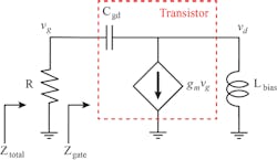
3. Here’s a low-frequency equivalent circuit of an RF/microwave PA with a biasing resistor.
Inserting a serial resistor to the gate-biasing network is a frequently used method to improve the stability. In this section, the contribution of the gate-biasing resistor to the low frequency stability is analyzed. Figure 3 shows the low-frequency equivalent circuit of a PA with a gate-biasing resistor.
If Eq. 4 is used to derive total impedance including the gate resistor, then Ztotal is:
Ztotal = R//Zgate = RZgate/(R + Zgate) (11)
Ztotal = [R(1 – ω2LbiasCgd)]/(1 – ω2LbiasCgd + jωRCgd – jω2gmRLbiasCgd) (12)
Since the frequency under consideration is in the megahertz range, the gate-drain capacitance Cgd is very small, and bias inductor Lbias is at a nanofarad value, the ω2LbiasCgd term in the numerator is smaller than unity. Therefore, Ztotal is almost equal to R for small values of R. For example, assuming that R = 10 Ω, a frequency of 200 MHz, Lbias of 10 nH, Cgd of 0.3 pF, and gm of 1000 mS, Ztotal = 9.9 + j0.44 Ω. However, this assumption is not correct for larger values of R. For example, if R = 1 kΩ, then Ztotal = 49.5 + j217 Ω.
Eq. 12 shows that a suitable bias resistor at the gate provides positive input resistance in the low-frequency region. While gate resistor R may seem to be a form of “magic” component for achieving low-frequency stability, the assumption is valid with an ideal RF bypass circuit. Microfarad- and nanofarad-valued capacitors tend to have high parasitic series inductance and resistance values, causing strong resonances in the low-frequency region. Any inductance of significant value due to an RF choke or a microstrip transmission line can affect the low-frequency resonances.
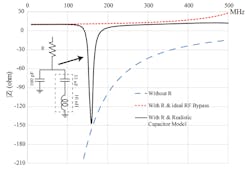
4. Input impedance variance of a SSD at low-frequency region; without resistor, with resistor, and ideal RF-bypass, with resistor and realistic component model (Cdg=23 fF/W, gm=30 mS/W [ref. 3], L=10 nH, R=10 Ω, P=30 W).
Figure 4 shows Zgate and Ztotal input impedances, with and without a gate-biasing resistor, and when considering real capacitor models (100 pF and 33 μF with 10-nH series inductance) instead of an ideal RF bypass capacitor. Strong resonances in the bias network can cause low-frequency oscillations in addition to reducing the video bandwidth and degrading the intermodulation-distortion (IMD) performance of an amplifier.
The structure of a PA biasing network will involve tradeoffs among stability, linearity, and complexity. Gate- and drain-biasing networks should contribute to improvements in overall performance and reliability. By understanding some of the essential rules for biasing networks, it is possible to achieve a desired compromise among the key design goals, including low-frequency stability, for an RF/microwave PA.
Seeking Stable Bias Networks
As has been shown, a series resistor in the gate biasing circuitry is a vital component for achieving low-frequency stability. The value of the resistor depends on a number of factors, including class of operation, saturation level, transistor technology, and device size. A smaller resistor may not have enough resistance to provide a wide-range positive input impedance. Conversely, a larger-valued resistor may cause undesired resonances and voltage swings on gate biasing due to gate current in different devices, such as in HEMTs.
A small amount of current, such as 1 to 2 mA, can flow down a transistor gate under the compressed operation of a high-power HEMT. The peak value of the gate current will depend on the SSD technology and will be proportional to the physical size of the SSD. For example, the gate current of a 100-W, 50-V GaN HEMT device is a few milliamperes.4 The voltage swing on the gate bias caused by a bias resistor changes the dc operating point of a PA, resulting in fluctuations in drain current and amplitude modulation of the signal.
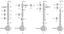
5. Frequently used gate-biasing networks for Ampleon PA demonstration PCBs.
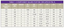
Figure 5 and Table 1 show some gate-biasing structures and component values for several power levels and frequencies commonly used for Ampleon PA demonstration boards. Fig. 5’s resistor-based biasing network “A” is suitable for under-1-GHz applications. Bias network “C” is well-suited for higher-frequency applications. In some cases, the gate-biasing network is also part of the impedance matching network, and bias network “D” is an example of that type of configuration. A shunt resistor, such as R2 in bias networks “A” and “C” in Fig. 5, relieves stability problems, but is not suitable for depletion-mode HEMTs due to their requirement of negative bias. A dc blocking capacitor, such as C2 in bias network “B” of Fig. 5, may be needed in some cases.
As shown in Fig. 4, the wideband response of all components in a gate-biasing network should be inspected for resonances. However, such an investigation can be cumbersome and sometimes impossible due to insufficient models of biasing components. A measurement-based analysis can be useful and time-saving, as will be shown in an example in which resonances are removed with the aid of S-parameter measurements and modeling.
The drain-biasing network influences the overall efficiency and RF performance of the PA directly. Moreover, extra attention is required during its design to increase the reliability of the PA due to the existence of the high voltage and current on the drain-biasing line. The dc, low-frequency, and high-frequency circumstances must be considered at the same time to achieve desired the PA performance, and stable and reliable operation.
The tradeoffs between these conditions shape the structure of a biasing network:
- The current-handling capability and dc resistance of its dc characteristics.
- The low-frequency stability and biasing induced memory effects of its low-frequency characteristics.
- The isolation and RF leakage of its high-frequency characteristics.
Eq. 5 shows that a larger value of the drain biasing inductance aids low frequency stability. But a narrower microstrip line is needed to increase the characteristic impedance of the biasing line for a larger inductance (Eq. 8). Decreasing the width of microstrip line increases its resistance and reduces its current-handling capability. A microstrip line with high dc resistance not only results in power loss and heating effects, but also a voltage swing at the drain, causing signal envelope distortion, PA linearity degradation, and asymmetry at adjacent channels. It complicates digital predistortion (DPD) efforts and can cause a failure in a DPD attempt.
Calculating the proper width and thickness of the microstrip used for the drain-biasing line by considering maximum current requirements is critical to achieving low inductance at low frequencies for improved stability, in addition to minimizing bias-induced memory effects5 and obtaining high impedance in the main operating frequency range for minimal RF/microwave signal loss. Table 2 offers a comparison of bandwidth, isolation, and heat dissipation in connection with the width of microstrip-biasing lines.
A wideband RF bypass at the drain-bias circuitry is also necessary to improve the performance of the bias network. For a wideband RF bypass, the drain biasing network usually includes a combination of capacitors with picofarad, nanofarad, and microfarad values. The picofarad capacitors provide low impedance at higher frequencies, while the other two values of capacitors are included for lower-frequency bypass and decoupling. Selection of convenient capacitor types and values is also essential to avoid undesired losses and resonances.6
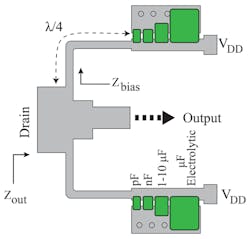
6. When a PA design’s PCB has sufficient real estate, a dual-biasing network can be used, as shown here with the PA’s output stage.
Several methods are available to increase the current-handling capacity of the biasing line. With adequate space on the printed-circuit board (PCB), a dual-biasing network can be used to decrease the total inductance at low frequency and increase current-handling capability (Fig. 6). Reduction of dc resistance, with negligible change in microstrip characteristic impedance, can also be accomplished by soldering a thin metal plate onto the microstrip line.7
The use of a shunt resistor-capacitor pair from drain supply point to ground in parallel with the RF bypass capacitors is another way to increase stability.8 The recommended resistor and capacitor values are around 50 Ω and 1 nF, respectively.
The RF bypass and decoupling capacitors at the biasing networks, particularly nanofarad and microfarad capacitors, may cause undesired resonances due to their low SRFs. Therefore, simulating the impedances and insertion losses of the input and output stages, including the biasing circuits from dc to at least the operational frequency range (f0) is required to discover any possible problems.
Unfortunately, such low-frequency-resonance analysis by means of computer simulation is often not feasible or accurate due to the lack of wideband models for nanofarad and microfarad capacitors. Therefore, S-parameter based measurements without SSD are useful and easy to determine the resonances.
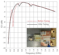
7. Measured |S21| values of the output stage before and after tuning of the biasing network, wideband S-parameter probe, and output stage (photograph).
Figure 7 shows the |S21| measurements of a PA output stage from the drain pad to the output. The PA is designed for a packaged two-stage GaN MMIC device at 2.14 GHz.9 A wideband microstrip probe was used for the measurements. The output stage was biased with a quarter-wavelength (λ/4) microstrip line, including RF bypass capacitors. At first, a strong resonance was observed around 340 MHz. After replacing the type X5R 10-nF capacitor with type X7R capacitor, and replacing the 180-nF capacitor by a 220-nF component, the resonance was eliminated.
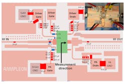
8. Layout view and components of the implemented PA.
Figure 8 shows the final circuit and its component values. Eliminating the initial resonance for this amplifier also extended its video bandwidth.
References
1. K.-W. Yeom, Microwave Circuit Design, Prentice-Hall, Englewood Cliffs, NJ, 2015.
2. S. C. Cripps, RF Power Amplifiers for Wireless Communications, 2nd ed., Artech House, Norwood, MA, 2006.
3. L. C. Nunes, P. M. Cabral, and J. C. Pedro, “AM/AM and AM/PM distortion generation mechanisms in Si LDMOS and GaN HEMT based RF power amplifiers,” IEEE Transactions on Microwave Theory & Techniques, Vol. 62, No. 4, 2014, pp. 799-809.
4. R. Baker, “GaN Power Amplfiier Bias and Decoupling Techniques,” IMS 2016 Microwave Applications, 2016.
5. M. J. Franco, “Bias induced memory effects in RF power amplifiers.” at: https://lintech.com.
6. R. Fiore, “Capacitors in Broadband Applications,” Applied Microwaves & Wireless, May, 2001.
7. L. B. Walker, Ed., Handbook of RF and Microwave Power Amplifiers, Cambridge University Press, Cambridge, 2012.
8. R. Basset, “High-power GaAs FET device bias considerations,” Fujitsu Compound Semiconductor Inc., Application Note, No. 10, 2008, pp. 1–7.
9. M. Acar, O. Ceylan, F. Kiebler, S. Pires, and S. Maroldt, “Highly Efficient GaN RF Power Amplifier MMIC Using Low-Voltage Driver,” in 47th European Microwave Conference, 2017.

