Move From Microstrip To Wide Slotline
Microstrip is the most common transmission line in microwave integrated circuits (MICs) and in companion with monolithic-microwave integrated circuits (MMICs). In contrast, wide slotline is not as widely used, but is easy to fabricate and preferable for many MIC and MMIC applications. For those applications employing wide slotline that also use microstrip, a transition is needed between the two transmission-line types.
A number of microstrip-to-slotline transitions have been developed and found useful in both academic and industrial fields.1-3 But one of the main difficulties is forming these transitions is achieving the match from the low impedance of microstrip to the high impedance of slotline.4 High-permittivity substrates and narrow slot gaps are often used to suspend the characteristic impedance of slotline, as well as to reduce the impedance difference between microstrip and slotline in forming a transition.5,6
Unfortunately, this technique is not always suitable for antenna applications. The high permittivity substrate can degrade an antenna’s radiation performance. In addition, fabricating the narrow slot gap is no trivial task. Some researchers have employed multisection impedance transformers to smoothly increase the characteristic impedance of a microstrip transmission line to the higher impedance of a slotline transmission line.7,8 But when such transformers are used with wide slot antennas, too many sections are required to achieve the desired impedance transition, resulting in a large and bulky design.
Fortunately, a novel transition design has been developed based on a dual branchline configuration. It is capable of achieving a low-loss transition between 50-Ω microstrip and 150-Ω wide-slotline transmission lines across a broad frequency range. The measured results for the back-to-back transition show better than 10-dB return loss and less than 3-dB insertion loss from 3.20 to 6.22 GHz—a 64% bandwidth. The transition design does not require either viaholes or airbridges. In addition, the transition can be etched on low-permittivity circuit material, making it a suitable candidate for integration with the feed networks of wide slot antennas and arrays.
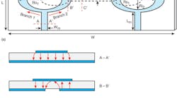
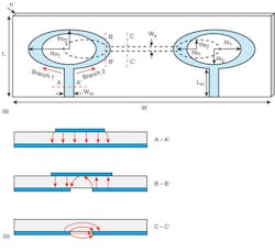
1. These sketches show (a) the geometry of the proposed MS-to-WSL transition as well as (b) the electrical field distributions at planes A-A', B-B', and C-C'.
Figure 1(a) shows an analysis model of the transition in its back-to-back form. It is based on a circuit substrate with thickness, h, of 1 mm, relative permittivity, εr, of 2.65, and circuit-substrate dielectric loss tangent, tanδ, of 0.003. The width, Wm, is set to a value of 2.85 mm to match the dimension common to 50-Ω SMA connectors. Width Ws is set equal to 1.5 mm with a characteristic impedance of 150 Ω. As Fig. 1(a) shows, branch 1 is C/2 longer than branch 2, where C is the outer circumference of the ellipse ring which can be calculated by the approximation:
C ≈ π[1.5(Ro1 + Ro2)] – (Ro1 Ro2)0.5
When C/2 = λg/2, where λg is the center guided wavelength, a 180-deg. phase difference is achieved between the two branches. Figure 1(b) plots the electrical field distributions at planes A-A', B-B', and C-C', respectively (at the center frequency). It is clear that the transition from the microstrip mode (A-A') to the wide-slotline mode (C-C') is mainly realized around plane B-B', where the two branches connect. The out-of-phase signals on the two branches excite in-phase signals on the wide slotline, in the process generating the wide-slotline transmission mode.
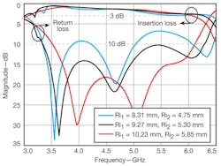
In addition to proper electromagnetic (EM) field matching, an effective transmission-line transition should ensure a smooth impedance shift for good wideband performance. Since inner axes Rig1 and Ri2 determine the width of the branches, they were studied with the aid of the ANSYS High Frequency Structure Simulator (HFSS) from Ansys to better understand their effect on the impedance matching of the transition. Figure 2 shows the return loss and insertion loss performances of the transition with different Ri1 and Ri2 values. To simplify the comparison, three set of values share the same axial ratio (Ri1/Ri2) of 1.75.
As Fig. 2 shows, insertion loss remains essentially unchanged with different Ri1 and Ri2 values, whereas the return-loss performance is sensitive to variations in Ri1 and Ri2. The return loss performance is degraded when the dimension of the inner ellipse decreases (correspondingly, with wider branch widths). One explanation for this is that significant reflection, due to mismatching, occurs at the T-junction where the parallel branches connect with the main line. When the dimension of the inner ellipse increases (correspondingly, with narrower branch widths), good impedance matching occurs at the center frequencies although the operating bandwidth tends to narrow. This is because the high quality-factor (Q) value in this case leads to a naturally narrower bandwidth.
2. These plots show the return-loss and insertion-loss characteristics for the microstrip-to-wide-slotline transition with different Ri1 and Ri2 values.
After fine-tuning and optimization, inner ellipses with dimensions of Ri1 = 9.27 mm and Ri2 = 5.30 mm were chosen as a compromise to achieve both acceptable impedance matching and relative wideband operation. In addition, the dimensions of the stub slots Rs1 and Rs2 were set to values of 6 and 3 mm, respectively, to better cancel the discontinuous effects of the wide slotline short end.
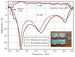
To evaluate the transmission-line transition concept, a prototype transition was fabricated on F4BK265 woven-glass PTFE substrate with relative permittivity of 2.65. The two-port transition was fed by means of 50-Ω SMA connectors. The prototype transition was evaluated by means of a commercial vector network analyzer (VNA), a Wiltron model 37296A (now available from Anritsu Co.). Measured results show better than 10-dB return loss and less than 3-dB insertion loss across the operating bandwidth, which was 3.20 to 6.22 GHz, or a 64% bandwidth.
Figure 3 compares the simulated and measured return-loss and insertion-loss performance levels for the transition. The jitter behavior of the measured insertion-loss curve might be attributed to irregular soldering. A frequency-offset of about 100 MHz cab also be observed between the simulated and measured return-loss curves. This is possibly due to the inappropriate quality of the microwave substrate. Otherwise, the measurements agree fairly closely with the computer simulations, validating the design concept for the microstrip-to-wide-slotline transition.
3. These plots compare the simulated and measured return and insertion losses for the microstrip-to-wide-slotline transition.
In summary, an effective microstrip-to-wide-slotline transition has been presented here. Elliptical ring-shaped branches and elliptical wide-slotline end stubs were employed; dimensions were optimized to ensure a smooth field transition and impedance transition between 50-Ω microstrip and 150-Ω wide slotline. The measured results for the transition show that it is capable of supporting operation from 3.20 to 6.22 GHz, a relative bandwidth of 64%. The transition was printed on a low-permittivity circuit substrate, making it a suitable candidate for integration with the feed networks of wide slot antennas and arrays.
Peng Fei, Doctor
Yong-Chang Jiao, Professor
Yang Ding, Doctor
Fu-Shun Zhang, Professor
National Key Laboratory of Science and Technology on Antennas and Microwaves, Xidian University, Xi’an, Shaanxi 710071, People’s Republic of China; e-mail (Peng Fei): [email protected].
References
1. R. Azadegan and K. Sarabandi, “Miniature high-Q double-spiral slot-line resonator filters,”IEEE Transactions on Microwave Theory & Techniques, Vol. 52, May 2004, pp. 1548-1557.
2. K. Song and Q. Xue, “Novel ultra-wideband (UWB) multilayer slotline power divider with bandpass response,” IEEE Microwave and Wireless Components Letters,Vol. 20, No.1, January 2010, pp. 13-15.
3. D.S. Woo, et al., “Broadband Antennas Using a Planar Ultra-Wideband Balun,” in International Conference on Communications Technology, Proceedings ICCT,November 2008, pp. 305-308.
4. K.C. Gupta, R. Garg, I. Bahl, and P. Bhartia, Microstrip Lines and Slotlines, 2nd ed., Artech House, Norwood, MA, 1996, pp. 305-313.
5. R.N. Simons, N.I. Dib, and L.P.B. Katehi, “Coplanar stripline to microstrip transition,” Electronic Letters, Vol. 31, No. 20, September 1995, pp. 1725-1726.
6. Y. Qian and T. Itoh, “A broadband uniplanar microstrip-to-CPS transition,” in Proceedings of the Asia–Pacific Microwave Conference, Vol. 2, 1997, pp. 609–612.
7. N. B. Wang, Y. C. Jiao, L. Zhang, Y. Song, and F.-S. Zhang, “A simple low-loss broadband 1-14 GHz microstrip-to-slotline transition,” Microwave & Optical Technology Letters, Vol. 51, No. 9, September 2009, pp. 2236-2239.
8. W.-H Tu and K. Chang, “Wideband microstrip-to-coplanar stripline/slotline transitions,” IEEE Transactions on Microwave Theory & Techniques, Vol. 54, No. 3, March 2006, pp. 1084-1089.


