Diode Quad Is Foundation For PIN Diode Attenuator
Download this article in .PDF format
Adjustable attenuators are useful in a variety of communications applications, for example, to control signal levels in receivers and transmitters. In particular, high linearity is a key requirement in many modern communications systems. By using a low-cost, SOT-25 surface-mount diode quad from Avago Technologies, it is possible to build a simple voltage-controlled attenuator with outstanding linearity performance over a wide frequency range from 0.3 to 3000 MHz. This type of attenuator is well suited for cable-television (CATV) networks and CATV set-top boxes, but is also useful in wireless and cellular communication infrastructure equipment in the very-high-frequency (VHF) and lower microwave regions, especially where limited space precludesthe use of distributed components.
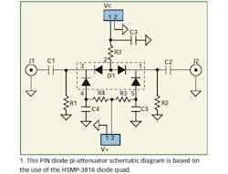
The model HSMP-3816 from Avago Technologies is a diode quad housed in a five-pin, lead-free SOT-25 surfacemount package. The pi-connected quad PIN diodes are adjacent die selected from the same wafer for closely matched electrical characteristics. In package form, pins 1 and 3 are assigned to RF input and output connections, pin 2 is used to provide series bias energy to the diodes, and pins 4 and 5 are used to supply shunt bias energy. In addition to the obvious size advantage, bundling four well-matched PIN diodes into one SOT-25 package helps ensure a more perfect symmetry between the attenuator's input and output arms than is realizable using physically distinct parts.
A basic pi-configuration fixed attenuator can be frabricated using two shunt resistors and a series resistor, which are set to achieve some desired value of attenuation A = 20 log (K) while simultaneously providing an input and output impedance which matches the intended application's characteristic impedance. When operated at a frequency well above its cutoff frequency, fc, a PIN diode can be used as a current-controlled variable resistor. However, this model is accurate only at frequencies well above the diode's cutoff frequency, fc = 1/2πτ , where is the minority carrier lifetime of the device. At frequencies 10 times fc, a PIN diode can accurately be modeled as a currentcontrolled resistance in parallel with a small (and constant) junction capacitance (neglecting package parasitics). At frequencies below 0.1fc, the PIN diode behaves as an ordinary PN junction diode.
For frequencies between 0.1fc and 10fc, the characteristics of the PIN diode become very complex; it will generally behave as a frequency-dependent resistance shunted by a very large frequency and current-dependent inductance or capacitance. Additionally, the distortion performance will usually be very poor when operating in this frequency range. For the HSMP-3810 series of diodes, τ≈1500 ns, resulting in a cutoff frequency of 100 kHz. This diode should therefore provide frequency-independent values of pure resistance at frequencies above 1 MHz. However, because this diode has been optimized for wideband attenuator applications, its characteristics remain generally well behaved down to frequencies below fc.
Three diodes can be used to replace the fixed resistors of the pi circuit to create a variable attenuator. However, the use of three diodes as variable resistors leads to asymmetry in the network, which results in a rather complicated bias network. Replacing the series resistor with two PIN diodes results in several performance benefits. First, since the maximum isolation of the network is set by the capacitive reactance of the series diodes, the use of two diodes in place of one will increase the maximum attenuation or double the upper frequency limit for a given value of attenuation. Second, the twin diodes which occupy the position of the series resistor are physically connected 180 deg. out of electrical phase, resulting in the cancellation of even-order distortion products. Third, the resulting attenuator network is symmetrical and the bias network is substantially simplified. Supply voltage V+ is a fixed voltage, and Vc is the variable voltage that controls the attenuation of the network. The only drawback to using two series diodes in place of one is a potential increase in insertion loss.
The four-diode pi attenuator requires a constant voltage, V+, and a variable control voltage, Vc. With V+ equal to 1.25 V, the variable control voltage will range from 0 V to about 5 V. The value of V+ represents a compromise between return loss and the required range of control voltage, with a lower value degrading the return loss at higher attenuation levels but permitting the use of a smaller range of control voltage.
The attenuator described in this article was implemented on an FR4-based printed-circuit board (PCB) with 8 mm thickness. While FR4 provides good mechanical stability and durability at low cost, it suffers from high losses and a poorly controlled and highly frequencydependent dielectric constant. On the other hand, fiberglass-reinforced polytetrafluoroethylene (PTFE) PCB materials can exhibit very good high-frequency properties, but are comparatively expensive. They also tend to have relatively poor mechanical stability and may not stand up to some surface-mount-technology (SMT) processing steps. Selecting a PCB substrate optimized for higherfrequency operation may improve performance at higher frequencies. The frequency dependencies of the various measured parameters are governed by the parasitics associated with the HSMP-3816 diode quad, PCB, additional required components, and connectors.
When PIN diodes are used as attenuating elements, they offer higher linearity than equivalent GaAs MESFETs. Distortion is minimized with the use of bulk PIN diodes with thick I-layer and low dielectric relaxation frequency (fdr). The HSMP-381x series has the thickest I-layer thickness in Avago's PIN diode product portfolio. At low attenuation, most of the RF energy is simply transferred from the attenuator's input to the output port. However, at higher attenuation levels, more of the RF energy is dumped into the attenuator and, consequently, the distortion level rises. When the value of Vc approaches zero, almost no current flows through the two series diodes. With these two diodes operating close to zero bias condition, their junction capacitance will vary in synchrony with the RF voltage. Fortunately, some of the distortion generated by the RF modulated capacitance will cancel out because of the two diodes' anti-series connection. The four diodes in one package concept ensure that the distortion cancellation is optimum as the two anti-series diodes are more closely matched than is possible-using two randomly picked diodes.
The phase shift through the pi attenuator varies with the attenuation setting. The total phase variation across attenuation is approximately 90 deg. and this remains reasonably constant when tested over three wide-spaced frequencies (100, 900, and 1800 MHz).
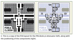
Fig. 1 shows a schematic diagram of the pi-attenuator circuit. The lefthand side of Fig. 2 shows the PCB layout for the pi attenuator, while the right-hand side of Fig. 2 illustrates the placement of components on the attenuator PCB.
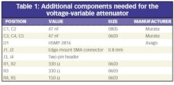
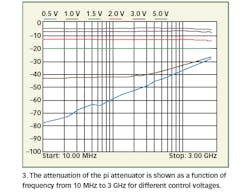
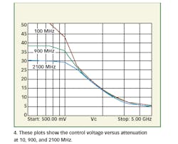
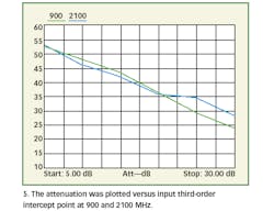
A listing of the parts required, including the diode quad, is shown in Table 1. Figures 3, 4, and 5 provide a sampling of the measured performance for a fabricated pi attenuator.
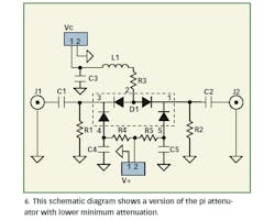
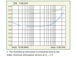
Increasing the bias current through the series diodes can lower the minimum attenuation limit. While maintaining a maximum control voltage of 5 V, the bias current can be increased by reducing the value of resistor R3. This can be achieved by adding surface-mount ferrite bead inductor, L1, in series with resistor R3 (Table 2) to provide RF blocking.
This ferrite bead inductor has higher impedance over a wider frequency range than a conventional ceramic-core, multilayer chip inductor. A schematic diagram for the circuit used for lower minimum attenuation is shown in Fig 6 A comparison of the standard attenuator circuit and the lowminimumattenuation circuit is shown in Fig. 7, at Vc=5 V.
In order to model the performance of the pi-attenuator design for further analysis, the Advanced Design System (ADS) computer-aided-engineering (CAE) software suite from Agilent Technologies (Santa Rosa, CA) offers engineers a support example to simulate the performance of the four-diode piattenuator design. The file can be downloaded from the "Examples" section of the Agilent EEsof Knowledge Center at www.edasupportweb.soco.agilent.com.
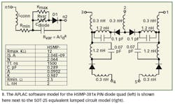
In addition, the PIN diode model contained in the APLAC CAE software suite of high-frequency modeling tools (www.aplac.com) can predict the RF resistance for a given value of forward bias. The left-hand side of Fig. 8 shows the APLAC model for the HSMP-3816 PIN diode.
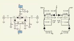
Combining the APLAC model with the SOT-25 equivalent circuit model (Fig. 8, right-hand side) allows the designer to account for the package parasitics in the simulation.
