This file type includes high resolution graphics and schematics when applicable.
1. The BAE Microelectronics Center (MEC) and its foundry houses people and equipment needed for the research and production of high-performance microwave, millimeter-wave, and even optical semiconductor devices, circuits, and modules.
Not every defense/aerospace electronics systems supplier can point to a full-fledged semiconductor foundry in its midst. But the Microelectronics Center (MEC) at BAE Systems is a full-featured, full-service compound-semiconductor foundry that can meet the company’s most challenging needs for high-performance, high-frequency semiconductors. The MEC can transform software design files into wafers full of high-performance, RF/microwave discrete and integrated-circuit (IC) semiconductors based on compound semiconductor materials such as gallium arsenide (GaAs) and gallium nitride (GaN).
The advanced facility doesn’t just enable BAE to design, fabricate, produce, and characterize its own semiconductor devices and modules. It also supports extensive R&D on new devices in support of internal and external customers’ needs for a wide range of electronic applications, including in avionics, electronic combat, communications, surveillance, and targeting systems.
The BAE MEC (Fig. 1) encompasses a total area of 70,000 ft.2, including 12,000 ft.2 of Class 100 IC fabrication clean-room space, as well as Class 10,000 and 100,000 clean rooms for the qualification of advanced high-frequency semiconductor devices and the assembly/test of higher-level MMIC-based assemblies. The facility features extensive environmental control equipment—like air-handling and filtration and gas-monitoring systems—to ensure the highest levels of cleanliness and a pristine environment for maintaining high-quality, high-reliability semiconductor devices.
Also supporting the facility are automated-test-equipment (ATE) systems that include vector network analyzers (VNAs) with frequency extension well into the millimeter-wave ranges. The MEC has been accredited as a Category 1A Trusted Supplier by the U.S. Department of Defense (DoD) biannually since 2008.
The facility relies on in-house molecular-beam-epitaxial (MBE) reactors to grow pseudomorphic high-electron-mobility-transistor (PHEMT) and metamorphic HEMT (MHEMT) active device layers on GaAs semiconductor wafers. GaN starting wafers, sourced from carefully qualified suppliers, are grown on thermally conductive silicon-carbide (SiC) substrates by means of metal-organic chemical vapor deposition (MOCVD). The MEC can form device features as fine as 20 nm (as needed for high-frequency, high-speed applications) via electron-beam lithography; the facility has already developed and produced millimeter-wave semiconductors operating as high as 200 GHz (see table).
In addition to RF/microwave/millimeter-wave devices based on GaAs, indium phosphide (InP), and GaN, the MEC has also performed R&D for production of photonic and integrated optoelectronic devices and circuits, including optoelectronic integrated circuits (OEICs), focal plane arrays, and optical parametric oscillators (OPOs).
The facility added high-volume GaN module production capabilities in 2015, renovating the facility the following year for efficient co-location of staff working on R&D and production. This included those involved with material growth and wafer processing, as well as with device and module design, test, and manufacturing. Economies of scale in working with larger wafers began back in 2004 with 6-in.-diameter GaAs wafers for the production of GaAs pHEMTs and MESFETs. Through the use of automated wafer-handling systems, defects can be minimized and the benefits of high yields from these large wafers can be realized.
Customers are the beneficiaries of such high-volume semiconductor production, with cost reductions typically a function of increased yields. For mature semiconductor processes like GaAs—where applications for the devices are well-established, such as in receiver front-end amplifiers—large volumes of devices are needed for both commercial and defense systems. The BAE MEC has shown its capabilities to meet high-volume military requirements for GaAs devices, with nearly 1 million GaAs MMIC devices delivered for F-22 production applications. The facility expects to be able to handle similar high-volume requirements for GaN devices.
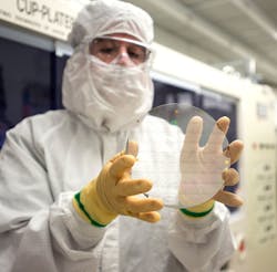
Although the GaN-on-SiC semiconductors are currently processed on 4-in.-diameter wafers, the cassette-to-cassette automated wafer-handling equipment used for 6-in. GaAs wafers has also been leveraged for the production of GaN-on-SiC devices on these smaller wafers by employing 6-in. wafer carriers, enabling BAE to achieve significant reductions in process defects and associated higher device yields. The semiconductor foundry facility has been evaluating device fabrication on 6-in.-diameter GaN-on-SiC wafers (Fig. 2) with excellent results. It expects GaN processing on these larger wafers to be ready for full production later this year.
BAE Systems, 95 Canal St., Nashua, NH 03064; (603) 885-4321
This file type includes high resolution graphics and schematics when applicable.


