Download this article in PDF format.
Advanced defense electronics systems often start with microscopic devices like semiconductors as building blocks, and that’s certainly the case with Northrop Grumman and its high-volume, high-frequency semiconductor foundry. In addition to selling semiconductor devices such as amplifiers and transistors fabricated in the foundry, the company offers foundry services for its gallium-arsenide (GaAs), gallium-nitride (GaN), and indium-phosphide (InP) wafer processes. Thus, customers can try their own monolithic-microwave-integrated-circuit (MMIC) designs on these state-of-the-art, high-volume microwave/millimeter-wave semiconductor processes.
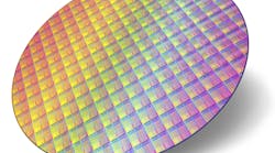
The high-volume semiconductor foundry (Fig. 1) constructs MMICs using heterojunction bipolar transistors (HBTs) and pseudomorphic high-electron-mobility transistors (pHEMTs), depending on the process. Each process starts with a 100-mm-diameter wafer, enabling customers to achieve a healthy volume of MMIC devices for a successful run. To improve the chances for a successful run, final design rule checks (DRCs) are performed by foundry personnel, who have more than a little experience on the requirements for each process.
1. The Redondo Beach, Calif. semiconductor foundry houses several different device processes for fabricating microcircuits with low noise figure, wide bandwidth, or high power at microwave and millimeter-wave frequencies.
The various foundry processes share a number of features, including availability of air-bridged metal and back-side viaholes for all processes, and the ability to implement Schottky diodes in all processes. As a DoD Trusted Foundry, the facility relies on mature computer-aided-engineering (CAE) models within leading software simulation tools, such as Keysight Technologies’ Advanced Design System (ADS) and the Microwave Office from National Instrument (NI)/Applied Wave Research (AWR), as well as extensive on-wafer measurement capabilities well into the millimeter-wave frequency range.
Picking a Process
Each semiconductor process has different benefits and limits—a designer can choose a process based on the design’s goals, such as low noise rather than high output power. Smaller transistor feature sizes will typically deliver higher transition frequencies (fT’s, the frequency at which device gain drops to unity) and higher maximum frequencies of oscillation (fmax’s), although usually with less power-handling capabilities for those smaller device features.
Four different InP processes are available, favoring power, high-speed digital, and low-noise/high-frequency (as in millimeter-wave circuits) architectures. All are fabricated on 75-μm-thick InP wafers The first three use Schottky diodes; the low-noise process employs gate-source diodes (Fig. 2). For example, the 1-μm TF2P power process achieves a peak fT of 80 GHz with peak fmax of 150 GHz and is specified for maximum collector-emitter/drain-source voltages (Vce/Vds) of 7.5 V dc.
2. This microphotograph shows a low-noise InP amplifier fabricated at the Northrop Grumman multiple-semiconductor-process foundry.
The 0.8-μm TF2 digital InP process, which offers a peak fT of 160 GHz and peak fmax of greater than 200 GHz, is tailored for maximum Vce/Vds of 5.0 V dc. For those in need of higher digital speeds and willing to operate with slightly less voltage, the 0.6-μm TF4 digital InP process reaches fT’s of greater than 250 GHz and fmax’s in excess of 300 GHz for maximum Vce/Vds voltage of 4.0 V dc.
When truly state-of-the-art digital speeds are required, the foundry offers its N60D 0.1-μm InP pHEMT process on 75-μm-thick InP wafers. The small feature sizes result in extremely low Vce/Vds of typically 1.2 V dc, but this is a semiconductor process capable of peak fT of 180 GHz and peak fmax of 350 GHz.
The semiconductor foundry’s diversity of GaAs pHEMT processes support a range of commercial through defense/military applications, spanning from cellular backhaul to millimeter-wave radars. For example, the 0.15-μm P3H GaAs pHEMT process is characterized by a peak fT of 80 GHz and peak fmax of 200 GHz while operating at 5 V dc. Designs are fabricated on a choice of 50- and 100-μm-thick GaAs wafers. The smaller-feature-sized P3K and P3D GaAs pHEMT processes are optimized for lower 4 V dc voltage, but provide higher fT of 120 GHz and fmax of 250 GHz.
When power is needed, the semiconductor foundry also offers its GAN20 0.20-µm GaN process for operation at 28 V dc. For applications such as power amplifiers and high-power oscillators, this process can leverage the higher supply voltages to a still respectable fT of 60 GHz and fmax of 200 GHz. The GaN process is fabricated on 100-µm-thick GaN wafers,
No matter the choice of semiconductor technology, the Northrop Grumman foundry backs it with the design, analysis, and test tools that help to achieve target performance goals, including in-house multiple molecular-beam-epitaxial (MBE) reactors. The foundry guarantees delivery of two 100-mm wafers per lot meeting target performance specifications, and will work with customers on how wafers are prioritized, offering multiple-project wafers as needed.
Northrop Grumman Systems Corp., Microelectronic Products & Services, One Space Park, Redondo Beach, CA 90278; (310) 814-5000, E-mail: [email protected].


