Accelerate PA Design with Source/Load-Pull ACPR and EVM Measurements
Download this article in PDF format.
With a rich set of load-pull data, power-amplifier (PA) designers can thoroughly investigate a device’s optimum capability in relation to design goals and performance targets. To fully benefit from this information, designers need an intuitive method to work with complex swept load-pull data sets. These data sets can include multiple fundamental frequencies, nested harmonic load-pull, and/or nested source- and load-pull.
As a result, PA performance becomes easy to understand across multiple operating conditions. In essence, performance can be analyzed in terms of frequency, power, and load or source impedance at the fundamental frequency and/or harmonic frequencies.
Measurements include available output power, gain, efficiency, and intermodulation-distortion (IMD) levels—essentially any performance metric that is able to be measured on a modern load-pull system. The measurements can be readily de-embedded to the current generator reference plane of the device, which is a critical consideration for any designer moving beyond the traditional reduced conduction angle classes of operation.
This article describes how load-pull data files with an independent swept parameter, such as power, can be used directly in the NI AWR Design Environment, specifically Microwave Office circuit design software. It also highlights the design of a Class J PA to show how load-pull data can complement traditional theoretical Class J analysis, thereby streamlining the design flow.
Background
Load-pull contours are acquired by sweeping the impedance presented to a device, measuring performance, and plotting the resultant performance data on a Smith chart (Fig. 1). As advanced load-pull measurement systems gain in popularity, increasingly sophisticated capabilities have been added to Microwave Office to help designers deal with ever-more complex load-pull data sets.
1. Load-pull sweeps the impedance of a device, measures the performance, and plots the resulting performance contours on a Smith chart.
Strategically using these tools ensures a streamlined overall PA design flow, enabling designers to eliminate guesswork and post-fabrication “tweaking” of first-cut prototypes (in the case of PCB designs). The same load-pull capabilities can be applied to simulated compact device models.
Device Model and Design Goals
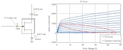
The example used for this article is based on Qorvo’s T2G6000528-Q3 gallium-nitride-on-silicon-carbide (GaN-on-SiC) high-electron-mobility transistor (HEMT). This device achieves approximately 10 W of output power at 3-dB gain compression (P3dB). It has a drain operating voltage (VD) of 28 V. The bias point is Class B or very heavy Class AB (Fig. 2).
2. Shown is the chosen device’s Class B behavior with the dynamic load line.
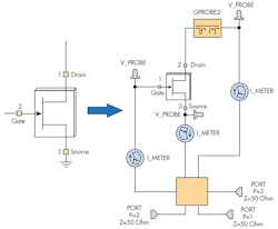
A Modelithics device model was used, enabling intrinsic IV sensing at the current generator plane of the device. This model allows a designer to “push down” into the model and make IV waveform measurements—not just at the package leads or transistor feed structure, where a typical, calibrated measurement system reference plane would be defined, but also at the device’s actual current generator right at the drain of the transistor (Fig. 3). The gamma probe element enables the user to actually plot the impedances directly at this critical reference plane.
3. The device model enabled the designer to make measurements not only at the package plane, but also at the current generator of the device, right on the drain pin of the die plane.
Introducing Nested Source- and Load-Pull Analysis
Microwave Office software simplifies designing with load-pull data by nesting together source- and load-pull results. Typically, when starting a device design, one needs to establish the appropriate source match before exploring the first-cut load-pull. Depending on the device’s level of reverse isolation (S12), a non-50-Ω load impedance will change the source impedance match. Therefore, designers should initially base their source match on the input impedance of the device when terminated with the preferred load impedance, which in turn is impacted by the source impedance.
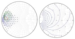
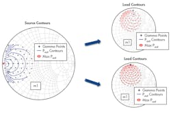
4. The impedance is selected on the source side (left), and the resulting set of contours is shown on the right side. Changing the impedance updates the load-pull contours.
Determining the optimum source and load impedances is therefore an iterative process. One way to streamline that process is to nest together source pull and load-pull, so that a load-pull data set contains both. For each source point there is a full set of load-pull data, and for each load point there is a full set of source-pull data. As shown on the left of Figure 4, the impedance can be selected on the source side. The right side of Fig. 4 shows the resulting set of generated contours. The impedance can be changed simply by moving markers, which updates the load-pull contours.
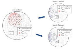
Conversely, on the device output, the load impedance point can be selected and the resulting source-pull contours can be seen (Fig. 5). Again, the source-pull contours are updated by moving the data marker amongst data points on the device’s load reference plane. This feature eliminates the need to perform iterative simulations with different source/load terminations in order to define the input and output target impedances—it is all there in one data set.
5. Changing the load impedance point on the load side (left) results in the source-pull contours shown on the right.
Load-Pull Multiple Performance Parameters
Once the initial source match is established, designers can focus on a more rigorous load-pull analysis. Any operating conditions, such as frequency or input power, can be taken into consideration. Rather than plotting strictly in terms of input power, data may be plotted in terms of other performance parameters like specific output power or gain compression points. Furthermore, as many data points as needed can be utilized.
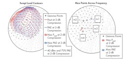
6. The oval shaped contour in the middle of the graph (left) is the overlap contour that meets two performance parameters at the same time. The maximum markers point out the maximum point for any measurement across frequencies.
In addition, Microwave Office offers an overlap contour, shown on the left of Figure 6. With the overlap contour, two performance parameters are being met at the same time. The graph on the right of Fig. 6 shows the maximum markers that point out the maximum points for any measurement across frequencies.
Class J Power Amplifier Overview
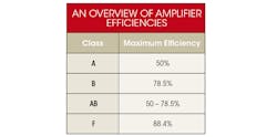
The table provides an overview of amplifier efficiencies. Approaching the shown maximum theoretical efficiencies depends on achieving a perfect short condition at the device’s current generator plane for harmonic frequencies. For Class F, the theoretical efficiency is actually 100%, where the voltage and current waveforms are “squared off” and 180 degrees out of phase. Theoretically, achieving this waveform shape would require shorting infinite harmonics, which is not practical. Thus, 88.4% is typically used as the maximum available efficiency achievable through the appropriate load impedances at the second and third harmonics.
Class J was introduced by Dr. Steven Cripps in 2006. It starts with a Class B bias condition and essentially adds the reactive termination at both the fundamental and the second-harmonic frequencies. Therefore, the linearity impairment is less than Class E, for instance, which is essentially a switched-mode operation.
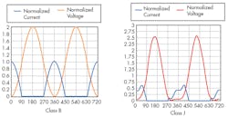
What does this mean in terms of the waveform shape? Figure 7 shows the Class B waveforms on the left and the Class J waveforms on the right.
7. Class B waveforms are shown on the left, with Class J waveforms shown on the right.
Class B has a 180-degree conduction cycle. For the Class J waveforms, some harmonic content was added. The current waveform is essentially squared off, minimizing the time when the device has a positive voltage and is conducting. The Class B theoretical efficiency can be reached without requiring short-circuit conditions, which allows for a much more practical approach.
Harmonic Load-Pull
How does this fit in with load-pull? Apart from fundamental load-pull, Microwave Office enables designers to perform load-pull analysis that includes load-pull contours based on termination impedances at harmonic frequencies. This capability allows designers to quickly assess the impact of controlling second- and third-harmonic terminations.
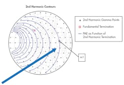
8. With harmonic load-pull, designers can evaluate the impact of controlling the second- and third-harmonic terminations. This capability makes it possible to determine where harmonic impedances can maximize device performance (blue arrow).
Figure 8 shows a fixed fundamental termination on the load side with the second-harmonic termination essentially being pulled around the entire Smith chart. Power-added-efficiency (PAE) contours can be plotted, which reveals the device’s efficiency based on its harmonic terminations and identifies an area of the Smith chart where efficiency is maximized.
De-embedding and Waveforms
De-embedding is important for studying the current and voltage waveforms at the device’s current generator plane instead of at the package leads. As noted earlier, the model used in this example enables designers to make measurements at the drain pin of the actual current generator of the device.
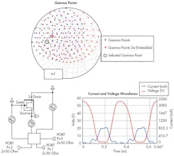
However, the model reference plane may not be at the current generator. If the designer knows the details of the internal matching elements, along with the package or test fixture (as represented by an S-parameter block), that knowledge can be applied in Microwave Office in the form of a de-embedding network. One can then plot the waveforms at the current generator (Fig. 9). Thus, the designer is able to directly determine if it’s achieving Class J conditions.
9. The de-embedded gamma points and waveforms are shown in this de-embedding network.
In the absence of either of these capabilities—a model or a de-embedding network—nesting can be used to sweep the fundamental, as well as second- or third-harmonic terminations, to obtain performance contours. This provides a useful design path when de-embedding isn’t possible or practical.
ACPR/EVM Load-Pull for Linearity
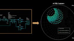
In the most recent release (V13) of NI AWR software, load-pull analysis was expanded to communication-system measurements via Visual System Simulator (VSS) co-simulation with Microwave Office. The new capability generates constant performance contours for metrics such as adjacent channel power ratio (ACPR) and error vector magnitude (EVM). This offers insight into amplifier linearity as a function of varying load conditions and how the device will operate under digitally modulated RF waveforms.
10. System measurements can be contoured to provide further impedance optimization, or to provide insight into the impact of varying load conditions.
In Figure 10, a quadrature-phase-shift-keying (QPSK) signal is applied. More sophisticated signals, such as LTE or 5G (also available in V13) modulated signals, can also be applied to plot communication-standard-specific contours. Fig. 10 shows plots of ACPR contours for the device.
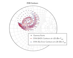
The new “system-based” load-pull offers the same functionality as using circuit-level load-pull with an expansion of measurements commonly employed in communication systems. As with circuit measurements, these system measurements can be referenced to a specific output power level or any other measurement—it doesn’t have to be just a function of the input power (Fig. 11).
11. As with circuit measurements, system-level measurements can be referenced to a specific output power level.
Conclusion
Load-pull is an integral part of high-power amplifier design, whether the source data is based on simulated load-pull device models or measured device-under-test (DUT) load-pull files. The unique functionality of nesting source- and load-pull contours in NI AWR Design Environment can significantly shorten the time required to design an amplifier—it streamlines the iterative process of optimizing the impedances presented to the device’s input and output terminals.
De-embedding and waveform plotting are critical for observing the matching circuit’s impact on waveform shaping (squaring off) to improve amplifier efficiency. When studying the waveform at the device model’s current generator is not practical, nested fundamental/harmonic load-pull contours can provide an alternative solution. Lastly, the addition of communication-system measurements to load-pull analysis adds a powerful design aid for engineers studying performance tradeoffs based on system measurements. Such measurements include ACPR and EVM for amplifiers operating with digitally modulated RF signals.
