Rectenna Serves 2.45-GHz Wireless Power Transmission
Download this article in .PDF format
Wireless applications inject a great deal of excess electromagnetic (EM) energy into the environment—energy which can be reused if properly recovered. A rectifying antenna, or rectenna as it is popularly known, is one such means for recovering that energy. In order to demonstrate the capabilities of such a design, a novel rectenna was developed for low-power operation at a single Industrial-Scientific-Medical (ISM) frequency of 2.45 GHz.
The rectenna consists of a highly efficient photonic-band-gap (PBG) structure, a microstrip lowpass filter (LPF) with defected ground structure (DGS) circuitry, and a Schottky diode. To evaluate the rectenna, it was fabricated on a low-cost FR-4 printed-circuit-board (PCB) material with relative dielectric constant (εr) of 4.4 in the z-direction at 10 GHz and thickness of 1 mm. As will be shown, the rectenna achieves RF-to-DC conversion efficiency of 63% when processing received power of +18 dBm at 2.45 GHz.
1. This diagram shows the main function blocks of the rectenna circuit.
Studies of wireless transmissions, and methods for preserving and conserving the power from those transmissions, have continued since the first wireless power transmissions (WPTs) by Nikola Tesla in 1899. Rectennas have been of interest for their capabilities to convert RF energy to DC power, and provide the opportunities to “reuse” some of this transmitted wireless power. In recent years, microstrip circuit technology has been widely used for the development of receiving rectifier antennas, with RF-to-DC conversion efficiency representing one of the most important parameters of any rectenna design.1-3
A rectenna is an antenna with additional components, including a LPF and a rectifying circuit. The rectenna receives microwave energy from the antenna.4-6 A Schottky rectifier diode converts the received RF energy to DC power.7-9 The amount of power that can be transmitted is limited, and the amount of RF/microwave power is reduced from the source through attenuation, mainly due to free-space signal path loss. For use in portable devices which, in generally, usually have small dimensions, an effective rectenna design should also have small dimensions.
In order to achieve higher-order harmonic rejection of unwanted signals, the rectenna design employs a miniature microstrip LPF with DGS.10,11 The simple DGS is applicable on 50-Ω feeder lines to achieve the requires lowpass filtering performance. The LPF with DGS can suppress and isolate second- and third-order harmonic signals from the rectifying circuitry, allowing the rectenna to achieve its target high RF-to-DC conversion efficiency without processing unwanted signals
Rectenna Design
Figure 1 shows a block diagram of the proposed rectenna design. In developing this design, the PBG antenna, DGS LPF, and rectifier circuits were all first designed, fabricated, and characterized separately. Then they were combined to realize a complete rectenna.
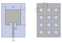
The linearly polarized PBG antenna was fabricated on 1-mm-thick FR-4 substrate with a relative dielectric constant of 4.4 at 10 GHz in the z-direction of the material (Fig. 2). The dimensions of the 50-Ω feed line were 20 × 1.9 mm. The dimensions of the PGB antenna were 30 × 31 mm. The photonic-band-gap (PBG) structure in the ground is designed to improve the gain and the directionality of the antenna. This increase in gain corresponds to improved power transmitting efficiency.
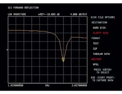
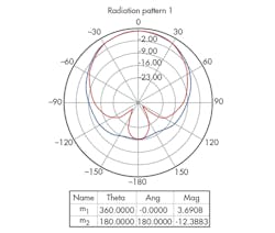
The square hole in the ground is designed for the PBG structure and it measures 6.6 × 7.0 mm. For some measure of the PGB antenna performance, Fig. 3 shows the antenna’s return loss while Fig. 4 offers its gain characteristics.
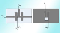
The rectenna’s DGS LPF was also designed and fabricated on FR-4 substrate material with relative dielectric constant of 4.4. With the U-slot added to it, the DGS offers good lowpass characteristics with improved harmonic-suppression characteristics in the high-frequency stopband. The proposed DGS LPF exhibits sharp filter cutoff characteristics, with low in-band insertion loss, wide stopband, compact size, and relatively easy fabrication. The U-shaped slot is combined with a rectangular groove measuring 3.8 × 5.5 mm and a pair of gaps measuring 0.50 × 7.25 mm.
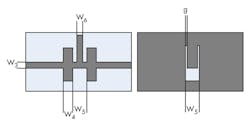
5. The schematic diagram represents the DGS LPF in the rectenna design.
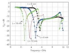
For enhanced performance from the LPF, symmetric stubs were introduced to increase the filter’s bandstop suppression in the high-frequency band. Figure 5 presents the structure of the DGS LPF used in the rectenna. The optimal dimensions for the DGS LPF are the following: W4 = 3.6 mm; W5 = 5.5 mm; W6 = 1.5 mm; and g = 0.5 mm. For good bandstop characteristics, the length of the symmetric stubs can be of great importance. As can be observed, the value of L greatly influences the band-notched frequency, as shown in Fig. 6. The bandstop frequency varies from 3.0 to 6.0 GHz as the value of L is varied from 0 to 18 mm.
A Closer Look
The commercial Schottky diode chosen for use in the rectenna design was a model HSMS-286C from Avago Technologies. This is a compact lead-free, surface-mount semiconductor that is usable from 915 MHz to 5.8 GHz. It features high detection sensitivity of as good as 50 mV/μW at 915 MHz, 35 mV/μW at 2.45 GHz, and 25 mV/μW at 5.8 GHz. The miniature surface-mount package helps save PCB space.In the rectenna design, the purpose of the rectifier is to directly convert RF/microwave energy into DC electrical energy. For this purpose, Schottky diodes are the preferred means of conversion for their low voltage drops and high-speed response and processing capabilities. In addition, Schottky diodes consume the least amount of power due to conduction and switching of alternative RF-to-DC conversion approaches.
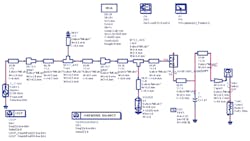
Within the rectifier circuit, the Schottky diode exhibits low parasitic circuit elements through about 6 GHz. High performance was achieved by modifying the basic parasitic circuit values and comparing them against the return-loss characteristics contained in the data sheet for the HSMS-286C. The main parameters for the HSMS-286C Schottky diode include series resistance, Rs = 5 Ω capacitance of Cj0 = 0.18 pF; and Vbr = 7 V. The next step was to create a matching input circuit for the diode, with matching done for the 2.45-GHz input. Figure 7 shows the simulated circuit module.
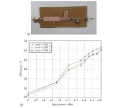
A matching circuit between the 50-Ω feed line and the RF-to-DC rectifying circuit is shown in Fig. 8(a). A peak efficiency of 63% was measured with a 250-Ω load and occurred at roughly +18 dBm received power, which is the maximum power rating of the diode. Loads of 200 and 300 Ω were also measured and produced nearly identical results. Figure 8(b) shows the conversion efficiency for the RF-to-DC rectifying circuit of these loads.
10. This test system was used to characterize the rectenna driving a single LED load.
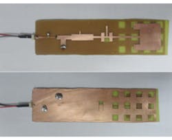
The rectenna shown in Fig. 9 was fabricated on a 1-mm-thick FR-4 substrate. It is designed to receive microwave energy in free space from a horn antenna with transmitted power levels to 4 W. The light-emitting diode (LED) is used as the low-power consumption load to verify the performance of the rectenna. Figures 10 and 11 offer glimpses of the test system used for this characterization. The rectenna was used to drive a single LED at a distance of 1 m and a voltage of +1.7 VDC. The energy received by the rectenna was +7.3 dBm. This translates to an efficiency of 13.9%. The rectenna also drove an LED array formed by three LEDs at a distance of 75 cm and voltage of +1.8 VDC. The efficiency of the rectenna in this case can reach as high as 45.5%.
11. This test system was used to characterize the rectenna driving an LED array.
The rectenna with PBG antenna operating at the single ISM-band frequency of 2.45 GHz represents a fairly simple design and an effective means of converting RF signals to DC energy at that frequency. The gain of the rectenna is 4.29 dBi at 2.45 GHz, with RF-to-DC conversion efficiency of as high as 63%. This particular rectenna design can operate effectively with low-power loads at these ISM frequencies using a low-cost LED to aid in the conversion.
This simple and straightforward conversion design can be applied to achieve power supplies for low-power loads, and can be useful in powering such applications as radio-frequency identification (RFID), wireless sensor network, and micro-mechanical systems.
Shuai Ji, Engineer
Hua Qi, Engineer
Huifeng Zhang, Engineer
The 20th Institute of China Electronics Technology Group Corp., Xi’an, People’s Republic of China
References
1. Hucheng Sun, Yong-xin Guo , Senior Member, IEEE , Miao He, and Zheng Zhong, “Design of a High-Efficiency 2.45-GHz Rectenna for Low-Input-Power Energy Harvesting,” IEEE Antennas and Wireless Propagation Letters, Vol. 11, 2012, pp. 929-932.
2. J.O. McSpadden, L. Fan, and K. Chang, “Design and experiments of high conversion efficiency 5.8 GHz rectenna,” IEEE Transactions on Microwave Theory & Techniques, Vol. 46, No. 12, December 1998, pp. 2053-2060.
3. W.-H. Tu, S.H. Hsu, and K. Chang, “Compact 5.8-GHz rectenna using stepped-impedance dipole antenna,” IEEE Antennas and Wireless Propagation Letters, Vol. 6, 2007, pp. 282-284.
4. Ugur Olgun, Chi-Chih Chen, and John L. Volakis, “Wireless Power Harvesting with Planar Rectennas for 2.45 GHz RFIDs,” 2010 URSI International Symposium on Electromagnetic Theory, 2010, pp. 329-331.
5. Z. Harouni, L. Cirio, L. Osman, A. Gharsallah, S. Member, and O. Picon, “A dual circularly polarized 2.45 GHz rectenna for wireless power transmission,” IEEE Antennas and Wireless Propagation Letters, Vol. 10, 2011, pp. 306-309.
6. U. Olgun, C.-C. Chen, and J.L. Volakis, “Investigation of rectenna array configurations for enhanced RF power harvesting,” IEEE Antennas and Wireless Propagation Letters, Vol. 10, 2011, pp. 262-265.
7. Y.-Y. Gao, X.-X. Yang, C. Jiang, and J.-Y. Zhou, “A circular polarized rectenna with low profile for wireless power transmission,” Progress In Electromagnetics Research Letters, Vol. 13, 2010, pp. 41-49.
8. G.M. Yang, R. Jin, et al., “Ultrawideband bandpass filter with hybrid quasilumped elements and defected ground structure,” Microwaves and Antenna Propagation, Vol. 1, No. 3, 2007, pp. 733-736.
9. J.S. Park, C.S. Kim, J. Kim, et al., “Modeling of a photonic bandgap and its application for the lowpass filter design,”Asia-Pacific Microwave Conference, Vol. 4, 1999, pp. 331-334.
10. Yasushi Horii and Makoto Tsutsumi, “Harmonic Control by Photonic Bandgap on Microstrip Patch Antenna,” IEEE Microwave and Guided Wave Letters, Vol. 9, No. 1, 1999, pp. 13-15.
11. S. Riviere, F. Alicalapa, A. Douyere, and J.D. Lan Sun Luk, “A Compact Rectenna Device at Low Power Level,” Progress In Electromagnetics Research, Vol. 16, 2010, pp. 137-146.
