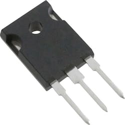
Non-Destructive Analysis of TO-247 Structural Defects
A single pulse of ultrasound fired into the polymer encapsulant of a TO-247 device travels through the polymer at a speed around 3,000 m/s. Its mission is to characterize any internal material interfaces that it encounters. It will be partly reflected by any material interface, but most strongly—virtually 100%—by the interface between a solid and an air gap, and less strongly by solid-to-solid interfaces.
When a pulse encounters a solid-to-solid interface, a portion of the pulse crosses the interface and travels deeper, where it may be reflected by a second interface. A solid-to-air interface reflects virtually 100% of the pulse, and no ultrasound crosses the interface.
The reflected ultrasound returns at its original speed to the receiver housed with the transducer that launched the pulse. Its round-trip time will be measured in nanoseconds. The returning echo can carry information about the depth of the interface, the acoustic impedance (density times acoustic velocity) of each of the two materials at the interface, and the change—positive or negative—in acoustic impedance in crossing the interface.
The instrument pulsing the ultrasound and producing the images is an acoustic micro-imaging tool. The images shown here were made by C-SAM tools in Nordson SONOSCAN’s laboratories.
Side View
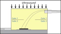
While scanning horizontally above the TO-247’s surface, the transducer repeats this routine many thousands of times a second, each pulse delivering information about interfaces directly below a single x-y location. Figure 1 is the diagrammatic side view of a TO-247. The row of arrows represents the thousands of pulses that the transducer will launch in each of many scans across the device. Echoes will be returned from interfaces between the mold compound and the internal features (leads at top right, die face, die attach, and heat sink) as well as from interfaces with air.
At a single x-y location, the information in the echo is turned into a single pixel in the acoustic image. An interface where a solid meets an air gap produces the highest amplitude echoes, which will be white pixels in the acoustic image, while the interface between two solids, where reflection amplitude may range from near zero to around 60%, is some shade of gray. If the pulse is fully attenuated before it can complete its round trip (unlikely in a TO-247), there will be no echo and the pixel will be black. In an acoustic image using a color map, any other colors can be used, although structural defects such as delaminations or voids are often shown in red.
Front View
In a TO-247, a completed acoustic image made from the front side will reveal the die, any extruded die-attach material around the die, any delaminations of the mold compound from the heat sink, any voids in the encapsulant, as well as the leads and the wires bonded to the leads. The leads are imaged separately because echo collection by the receiver is generally gated on (i.e., restricted to) a specific depth range of interest. A gate wide enough to encompass vertically both the leads and the die in a TO-247 would likely be out of focus at one of those depths.
Figure 1 shows approximately where each gate may lie. Except where they’re bonded (or not bonded), the wires produce few echoes because their curved surface scatters ultrasound in various directions.
Topside View
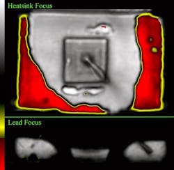
Figure 2 is the Gate 2 topside image of a TO-247 imaged by a 15-MHz transducer having a focal length of 0.75 inch. The die and much of the heat sink are within the image at the top of Figure 2. The most obvious defect is the red areas marking delaminations of the encapsulant from the heat sink. The delaminations may contain air or possibly a vacuum, both of which block ultrasound from crossing the gap, even if its vertical extent is a tiny fraction of a micron.
Acoustic evaluation of TO-247s and other high-power components considers the likelihood of expansion of structural defects. In this device, the delaminations are already substantial and could conceivably reach the die. Red was used to color them because the the air-to-solid (mold compound) produces the highest possible echo amplitude (>99.9%). Red is at the bottom of the color map along the left side of Figure 2.
Red regions mark negative reflections, where the pulse encounters a material of higher acoustic impedance (= density × acoustic velocity) followed by a material lower acoustic impedance. In this color map, the reverse situation—positive polarity—would be white.
There are additional defects above and below the die. The white features aren’t voids but rather excess—a foreign substance that somehow was incorporated during assembly of the device. They’re white because an arriving pulse went from a material (mold compound) of lower acoustic impedance to a material of higher acoustic impedance. This reflection has positive polarity.
The lower feature has a tiny red void next to it. The upper feature has a tiny area that appears red, not because it’s a void, but because the curved surface of the excess die-attach material is round enough to scatter the arriving ultrasound.
Using a shallower gate (Gate 1), the leads to which the wires from the die are attached were also imaged (bottom of Figure 2). The wire at left has the desired image: a light region near the edge of the lead, and a darker region below it. The light region indicates good bonding. The wire on the lead at right may be less securely bonded, although there are no red areas that would indicate an air-filled delamination.
Back View
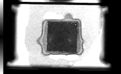
The TO-247 was then flipped right to left and imaged from its back side, through the heat sink (Fig. 3). Most of the regions that are red in the front-side image are white here because a grayscale color map was used. Gray areas are well-bonded. A few tiny voids are also in the die attach.
Imaging Another TO-247
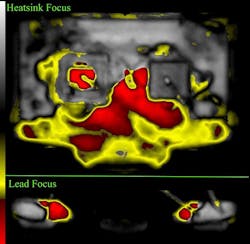
The top view of a second TO-247 (Fig. 4) was also imaged at 15 MHz by a transducer having a focal length of 0.75 inch. The die at left, which is somewhat obscured, is slightly larger in area than the die at the right. The red regions are delaminations of the mold compound from the heat sink and (at left) the die. Yellow regions may be partially bonded or may be tilted. Both conditions will reflect slightly less ultrasound than the fully delaminated regions. In a high-power device, defects of this magnitude make early field failure very likely.
The two leads are imaged at the bottom of Figure 4. The wire at far right has the same appearance—a pale region near the edge—as the leftmost in Figure 2 and is likewise well-bonded. But the red regions around the two other wires reaching these leads show that they’re poorly bonded or not bonded at all.
The acoustic images in this article were made with the commonly used C-mode imaging method. Over a dozen other acoustic imaging modes can produce, for example, a non-destructive cross-section; up to 100 or more thin gates at progressive depths within the sample; a three-dimensional acoustic image; a variably sectionable three-dimensional image; or any of several other image types. Their value for TO-247s lies in identifying fabrication errors and in preventing defective devices from going into service.
Tom Adams is a consultant at Nordson SONOSCAN and Enes Ugur is a member of the Power Electronics and Drives Lab at The University of Texas at Dallas.

