Members can download this article in PDF format.
What you’ll learn:
- The three categories of power-delivery network noise.
- Some tips for accessing PDN signals.
- Probes matter: Use the right probe for your application.
Power integrity is of critical concern for embedded-system designs, extending from a power-distribution network’s (PDN) power rails on a printed circuit board to its integrated circuits. Taking steps to maintain power integrity will ensure that voltage noise levels remain within the tolerances required for the various devices that make up your design.
As a rule of thumb, logic components can tolerate disturbances of 5% of the rail voltage. For higher-speed digital components such as transceivers, tolerance drops below 5%, while for mixed-signal, analog and RF components, tolerance drops below 1% of the rail voltage.
A typical embedded system incorporates a microcontroller and peripheral components including memory and I/O, with each component powered by a voltage-regulation module (VRM) that gets its power from a bulk supply. In addition, an embedded system includes interconnects, traces, planes, and decoupling capacitors, all of which can affect power integrity.
Noise Categories
There are three categories of PDN noise: self-aggression noise, board interconnect pollution, and mutual-aggressor noise.
An example of self-aggression noise is that which a VRM induces on its own output. To measure self-aggression noise, you must eliminate other sources of noise—ideally, the rest of the system will be in a known quiet state. Figure 1 shows a 900-mV rail with no load on the VRM, and you can see the switching noise and ripple—a relevant figure of merit.
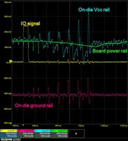
You also can observe the self-aggression noise of VCC, as shown in Figure 2, where the blue trace represents the on-die VCC rail. The green trace represents the board power rail; you can see that the board power rail and VCC noise is correlated but not identical. One noise source is I/O-driver switching, with one I/O signal represented by the yellow trace. A key takeaway here is that observing a small amount of noise on the board power rail doesn’t guarantee that there isn’t a lot of noise inside the integrated circuit.
The next category is board interconnect pollution. An example is the appearance throughout the PDN of VRM switching noise. I/O switching can cause noise pollution, too. In addition to showing VCC noise, Figure 2 also shows the on-die ground rail. When I/O signals switch, they create current flow in the return path, which in turn induces voltage changes on the ground rail.
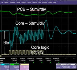
Figure 3 illustrates the impact of logic-switching activity on both the board power rail and core power rail, indicated by the green and blue traces, respectively. Clearly, the noise on both traces is correlated to the core logic activity. Note that the core noise is a much larger amplitude than the board noise. This is caused by a non-ideal PDN impedance profile.
The PDN connects to potentially every system component, and problematic noise coming from one place can spread everywhere. The measurement challenge is to determine which component or phenomenon is causing the observed noise; then, you can take on its mitigation. The most effective way to do that usually involves using a spectral approach to identify problematic aggressors. In an oscilloscope, one would typically use a fast Fourier transform (FFT) math function or a spectrum-analyzer software package.
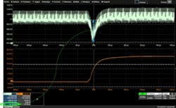
The last noise category, that of mutual aggressors, includes coupling from the PDN back into the components. If a component turns on and applies a load step to the VRM driving that component, the VRM will require time to react, and during that time there will be some noise. Figure 4 shows a current step and the resulting VRM output voltage dip before recovery.
You can also get crosstalk coupling from the PDN onto I/O signals. For example, say you have voltage noise on the PDN that’s shifting the threshold of a high-speed transmitter, and the signal being clocked out has a non-zero transition time. In such a circumstance, any shift up or down to the threshold becomes a corresponding shift in the timing determined by the slew rate of the signal.
That threshold shift will cause the signal edge to clock slightly earlier or later than expected. The impact to the circuit could be a rather large increase in clock jitter, leading to problematic system operation.
Accessing Signals
When choosing a probe to access power-rail signals, keep five considerations in mind:
- The signal of interest is usually a small disturbance riding on a larger voltage, so you will need to ensure the measurement system noise doesn’t swamp out the signal of interest.
- If you’re measuring high-frequency content, then any impedance discontinuities in your measurement path can cause reflections, distorting the content of interest.
- Ensure that your measurement system provides sufficient offset to match the rail voltage without compromising the signal-to-noise ratio (SNR).
- Many power-supply noise signals (including ground bounce and crosstalk from serial-data signals) have high-frequency content, so make sure your measurement system has adequate bandwidth to capture and characterize them.
- Note that low-impedance probing options can cause unacceptable loading on the PDN.
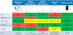
You can choose from five common probing options for power-rail measurements. First is the 10-MΩ passive probe—the type that comes with most oscilloscopes. This probe has 10X attenuation, resulting in a 10X reduction in SNR compared to some other probing options, but it is low cost, its loading is low, and it is unlikely to cause reflections.
Another option is to include a coaxial connector on your board and connect that directly to a 1-MΩ oscilloscope input. This one-to-one probing option keeps noise and loading low, although reflections may occur if you’re observing a signal with high-frequency components because of the transition from the 50-Ω coaxial environment to the 1-MΩ oscilloscope input.
A third option is to connect the coaxial connector on your board to a 50-Ω oscilloscope input. This approach offers high bandwidth with little reflection. However, presenting a 50-Ω load to the PDN could be problematic.
A fourth option is to build or buy a 10:1 coaxial probe. This approach similarly offers high bandwidth with little reflection, although the 10X attenuation will reduce your SNR. This option offers moderate loading at 450 Ω, which should be suitable for many PDNs.
The fifth option is the gold standard—a voltage-rail probe, such as the Teledyne LeCroy RP4030. That probe offers bandwidths up to 4 GHz, and it’s specifically designed to present a 50-kΩ load at dc, so the PDN doesn’t see a significant low-impedance load. At higher frequencies, it transitions to a 50-Ω load, minimizing reflections and distortion. It also contains a built-in offset digital-to-analog converter (DAC) to permit the maximum offset adjustment to view small voltage changes on dc power rails.
Figure 5 shows a summary table comparing the five different probing options.
Measurement Examples
Several examples illustrate some specific power-integrity measurements. First is rail transient response, measured using an active voltage-rail probe and a current probe. (Alternatively, you can measure current by measuring the voltage across a shunt resistor.) The goal is to measure steady-state rail behavior prior to a load being applied (mean voltage and ripple amplitude), step response (droop, recovery time, and settling time) and steady-state rail behavior after the load is applied.
You can make these measurements using cursors. To measure droop, for example, you can place the cursors at the observed mean rail voltage level and the observed negative peak, as shown in Figure 4. This approach isn’t very precise, though. Zoom traces can provide better visibility into high-frequency behavior while limiting parameter measurements to subsets of the acquired waveform.
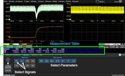
An alternative is to use power-integrity and digital power-management application software designed to simplify this type of analysis. Teledyne LeCroy provides such software that can use a synchronizing signal—such as a VRM’s clock signal—to enable per-cycle measurements and analysis. The software provides easy access to commonly measured parameters including RMS values, standard deviation, mean, peak-to-peak, positive peak, negative peak, and frequency, and it can present them in tabular form (Fig. 6).
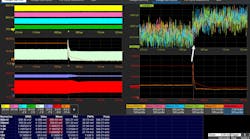
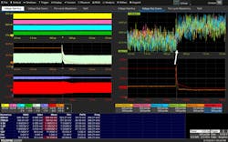
Another example is multi-rail analysis. In Figure 7, the power rail represented in light green on the left middle grid experiences a load release, signified by the current waveform transition (orange trace on the left). Clearly, the rail experiencing the load release exhibits a transient response, but the question arises: Do other power rails represented by the four traces at the top left experience any effects?
With the synchronizing signal used to derive the mean per-cycle voltage values of the four other rails, the digital power-management software generates the plot on the top right. It shows that the other rails do change, but by less than a millivolt.
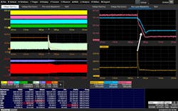
Figure 7 also illustrates the bulk 12-V supply (purple trace, lower left), which appears to experience reduced noise after the load release, based on the change in thicknesses of the trace before and after the load release. The digital power-management software can help quantify that. Figure 8 shows that the 12-V supply’s standard deviation (pink trace, top right), which is related to RMS noise, drops significantly from about 80 mV to about 25 mV after the load release.
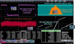
A final example focuses on rail-noise-induced jitter with a wireless router as the device under test (DUT). The blue trace (upper right) in Figure 9 is a 500-µs acquisition of a 10-MHz clock on the DUT. The red trace (lower left) is a time-correlated plot of time-interval-error (TIE) jitter measurements of the 10-MHz clock vs. time. The software compares the actual clock signal with an ideal one, performing a TIE measurement for each transition to determine how early or late each edge arrives.
The orange histogram (upper right) is a display of the statistical distribution of all TIE jitter measurements shown in the red trace. Software derives the jitter spectrum of the TIE values (not the vertical noise values) in picoseconds (lower right trace), with the largest value of 9.9 ps appearing at 2.956 MHz, as shown in the table in the lower right portion of Figure 9.
The conclusion is that the biggest contributor to power-rail noise is clock jitter occurring at 2.956 MHz. Eliminating the source of this clock jitter could significantly reduce power-rail noise.
In summary, understanding the potential sources of embedded-system noise and knowing how to choose the optimal probe for measuring it can help you maintain power integrity throughout your design. A recent webinar1 provides more details and is the first webinar in an 8-part Power Integrity Masters Series.
Reference
Connally, Patrick, Fundamentals of Power Integrity, June 2, 2021. https://teledynelecroy.com/events/.
