An Introduction to S-Parameter Network Flow Diagrams
This article is part of the TechXchange: Vector Network Analyzers.
This is the second in a multi-part series of articles on vector network analysis. Part 1 introduced the VNA, how such instruments work, and some of their applications in the lab.
Engineers should be familiar with the solution of Telegrapher’s equation for RF signals on a transmission line. That is:
where the transmission line is oriented along the x axis. It shows that a transmission line will support RF propagation in both directions simultaneously. The first term represents a wave moving in the positive “x” direction, and the second represents a wave moving in the “-x” direction. Because these two waves can be separated and measured by a vector network analyzer (VNA), they may be considered separately. S-parameter network flow diagrams do just that.
What Makes Up an S-Parameter Network Diagram?
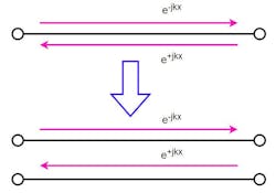
The first step in the graphical transformation is shown in Figure 1. Signals flowing in each direction are shown in separate paths, with signals moving from left to right on the top and those moving from right to left on the bottom.
Next, we account for reflections by adding arrows, which allow for a portion of a signal moving in one direction to be channeled to the other direction, transferring from the bottom of the diagram to the top or from the top to the bottom. These are the vertical arrows shown in Figure 2.
The actual voltages have also been replaced with S-parameters, which represent the relative amplitude and phase of the voltages with respect to the incoming stimulus signal. The nodes where reflections occur have been labeled with “a” and “b” designations. The “a” nodes may have signals entering them from outside the network, and the “b” nodes have signals exiting the network. This is a convention, but it needn’t always be the case.
Note that although the diagram of Figure 2 looks like a ladder network with two ports on each side, it’s nothing of the sort. There’s only one actual RF port on each side, each one with two contrived nodes—one for the forward wave and the second for the reverse wave. Network flow diagrams are discussed in some detail in References 2 and 3 (see below).
How Can the Diagram be Manipulated?
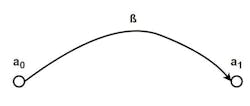
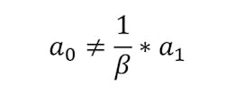
The network diagram shows signals traveling in only one direction. The mathematics of network analysis must take this into account. Figure 3 depicts a single flow connection. Here, it can be said that a1=β*a0.
The math works only in the direction of the arrow, so:
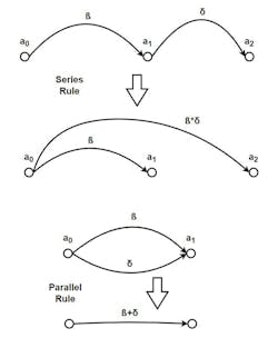
With this simple rule in mind, one may derive all other rules of diagram manipulation. The first two, series and parallel rules, are as shown in Figure 4.
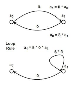
For two signal paths connected in parallel but with opposing directions, the parallel rule doesn’t apply. Thus, one must consider the two equations represented by the arrows. Figure 5 shows this condition.
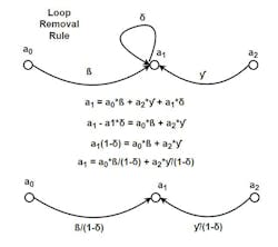
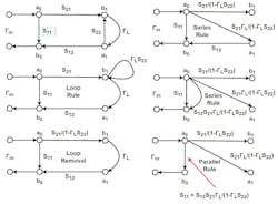
One of the signal paths is replaced with a “loop.” Resorting to another simple calculation, a loop may be removed by modifying all signal paths that enter it (Fig. 6). A loop will always have at least one signal path entering it and signal paths leaving a loop aren’t altered.
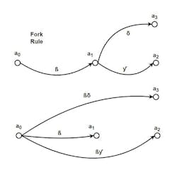
Finally, consider the case of forking signal paths. The simplification uses the series rule twice, as shown in Figure 7.
The point of all of these transformations is to arrive at a diagram where every node is a function of a single independent input node, or the driven node a0, in these diagrams.
A Practical Example
We can look at the simple example of a device with known S-parameters loaded with an arbitrary load ΓL as in Figure 8. We want to simplify the network such that every node is a function of a0 alone.
After this is achieved by applying the rules given earlier, the input reflection coefficient of an S-parameter network loaded by ΓL has the familiar result:
This result makes intuitive sense. If the isolation S12 is small, the load will have little effect on the input of the network, and one will measure S11. If the load is 50 Ω, then ΓL is zero and again one measures S11 at the input.
Much longer networks may also be collapsed into this more deterministic form. There isn’t much need to manipulate S-parameter networks in this way. But being able to do so provides an intuitive understanding of their function, which will be helpful for understanding the 12-term VNA error model. This model and a few others are essential parts of the calibration repertoire.Conclusion
Network flow diagrams are a useful tool to analyze systems and devices characterized by S-parameter matrices. The diagrams promote an intuitive understanding of the interaction of the voltage waves moving in each direction. In the next article of this series, we will introduce 8- and 12-term vector-network-analysis error models expressed as a network flow diagram, which are helpful to interpret where the errors occur and what they mean to the measured result.
Read more articles in the TechXchange: Vector Network Analyzers.
References
1. Mason, Samuel, “Feedback Theory – Further Properties of Signal Flow Graphs,” Proceedings of the IRE (Volume: 44, Issue: 7, July 1956).
2. Jim Stiles, University of Kansas, Dept. of EECS, “4.5 – Signal Flow Graphs,” 3/19/2019.
3. Feim Ridvan Rasim, Sebastion M. Sattler, “Analysis of Electronic Circuits with the Signal Flow Graph Method,” Scientific Research Publishing, Circuits and Systems, 2017, 8, pp. 261-274.
