Download this article in .PDF format
Noise can not only degrade the performance of electronic equipment, it can also prevent new electronic equipment designs from passing compliance testing. A combination of factors, such as increasing digital processing speeds, shrinking electronic package sizes, and more densely spaced electronic components, are contributing to increased amounts of electromagnetic interference (EMI) and radio-frequency-interference (RFI) noise, and boosting the needs to understand such noise sources and how to protect against them. Fortunately, as noise sources have become more complex, filtering solutions, such as filtered connectors, have been developed to help keep EMI and RFI in check.
Unwanted noise such as EMI and RFI can degrade the performance of communication and computing systems and cause false triggering and faulty readings in vital sensor circuits, resulting in system failures. Such noise can also cause incompatibility and compliance problems between different commercial, industrial, and military systems, resulting in noncompliance between those systems. As a result, engineers must be fully aware of and address the needs for EMI, RFI, and even electromagnetic-pulse (EMP) protection during the design and test phases of a project; various operating conditions, such as transient voltage surges, can result in elevated EMI and RFI levels. Being aware of possible problems from EMI, RFI, and EMP can help avoid failing compliance testing for a new product, and the costs of redesigning and retesting the electronic systems and components for that product.
EMI suppression is often handled by filters designed to meet the increased performance demands levied during testing from various standards, such as MIL-STD-461, RTCA-DO-160, CISPRE, and CE marking (formerly EC or European Conformity) in European countries. The trends of increased EMI/RFI noise from electronic products has led to the need for multiple shielding approaches and higher performance filters.
One of the problems in controlling EMI is that although electronic and mechanical system and component designers are well versed in the engineering problems of their respective areas, layouts required for electromagnetic compatibility (EMC) may be somewhat new to them. They may be unfamiliar with the particulars of the design/test compliance requirements, or are unaware of the costs associated with failing compliance testing and resulting redesign costs for their devices. Even without failures, it may cost $50,000 (US) to fully test and certify a device, including all required environmental and EMI compliance testing. Failing the test parameters may end up costing twice as much.
Four approaches are available to handle EMI/EMC filtering requirements. Filtering can be designed into a printed-circuit board (PCB) or device during the initial engineering phase. Or filtering can be added after a product’s initial design stage by means of three devices: (1) filter inserts, installed in front of device connectors, (2) filtered connectors, with a filter contained within the device connector, and (3) filter/transient-voltage-suppression (TVS) interface modules.
1. Filter inserts represent a low-cost, practical solution for many EMI/RFI problems.
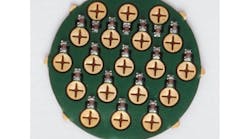
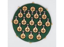
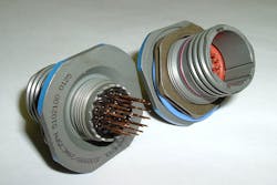
Filter inserts (Fig. 1) are generally considered the lower end of the spectrum in terms of cost and filtering limitations, although they represent a very practical solution for many applications. It is a simple and quick solution in which a filter can be added to a component or system to determine whether the level of filtering it provides is sufficient to solve the EMI problems. The filter connector (Fig. 2) is a somewhat more-elegant, higher-performance approach to controlling and eliminating EMI/RFI noise. It is more expensive than a filter insert, but is available in a much wider range of configurations and mounting arrangements and can include additional components as required, such as chip capacitors and TVS components.
2. Filter connectors can be supplied in a wide range of configurations to control EMI and RFI.
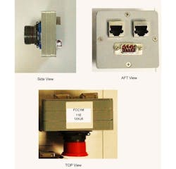
Filter modules are add-on components attached to an existing design, and are available with or without TVS capability (Fig. 3). Some of the advantages of using filter modules include more sophisticated filtration, avoidance of the need to insert additional PCB design integration into an already functioning fielded unit, and avoidance of the costly time required to change a design layout and retest circuitry.
3. Filter modules are sophisticated EMI/RFI filtering approaches and can be supplied with additional components.
In addition, customized solutions may be required to meet some EMI/RFI filtering requirements. Such solutions may involve design consulting, troubleshooting, device modification, and pre-certification testing to determine the level of modifications that might be needed to help a product achieve proper EMI/RFI levels for certification. Some companies that supply EMI filtering products also offer designing and re-engineering services to help with EMI/RFI problems, and these services, performed by experienced staff can greatly reduce the time and expense that might otherwise be required to overcome EMI/RFI problems.
Brett Robinson, Director of Engineering
EMI Solutions, Inc., 13805 Alton Parkway, Irvine, CA 92618; (949) 206-9960, Fax: (949) 206-9983; E-mail: [email protected], www.4emi.com.


