Download this article as a .PDF
Practical semiconductor devices at millimeter-wave frequencies will be needed to enable the realization of the many small cells with high-data-rate capacities for Fifth Generation (5G) wireless communications networks. Part of developing those high-frequency, high-speed devices will be testing them during design and development and then in production. The TS150-THZ manual probe system from MPI Corp. has been designed for on-wafer measurements not just through the entire millimeter-wave frequency range, but at terahertz (THz) frequencies as well.
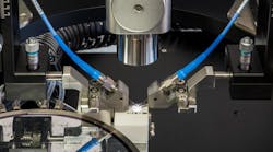
The TS150-THz manual probe system (Fig. 1) is designed for benchtop use, with easy access to a device under test, such as a semiconductor wafer. It is well suited for four-port S-parameter measurements with a high-frequency vector network analyzer (VNA). It has a low-profile configuration with a large, rigid platen, providing enough room for large-area micro positioners for maneuvering test probes for measurements from RF through terahertz frequencies.
The system is also well suited for optical and impedance-related load-pull measurements. In addition, it accommodates mounting of several of the high-frequency extenders used with VNAs for testing at millimeter-wave and terahertz frequencies.
The TS150-THz probe station features a vibration-absorbing base and a four-port bridge designed to simplify access to DC biasing and four-port RF measurements. The unique platen is made of nickel-plated steel and has three discrete lift positions for probe contact, separation, and safety loading of a DUT. The probe station is designed not only to perform repeatability measurements, but to ensure the long operating lifetimes of test probe tips.
For example, an “auto contact” position function moves the probe tip to the contact pads on a DUT with ±1 μm repeatability. In addition, the separation (from the contact point) repeatability is also within ±1 μm, ensuring that all mechanical positioning conditions during wafer probing remain consistent.
The x-y-z positioning of the chuck is performed with great position, and with respect for the mechanical and electrical requirements of making probe contacts to microscopic DUTs at such high frequencies. Positioning is achieved with the aid of a puck-controlled air bearing stage which is capable of rotational (theta) positioning of 360 deg. with a fine theta travel range of ±5 deg. The theta settability resolution within this fine travel range is 7.5 × 10⁻³ gradient with less than 10 μm planarity.
The chuck x-y stage has a total travel range of 180 × 300 mm with a fine travel range (for precise positioning) of 25 × 25 mm. The x-y positioning resolution in this fine-travel range is better than 1 μm. The chuck z-dimension stage has a travel distance of 10 mm with better than 1-μm adjustment resolution.
The precision and accuracy provided by the probe station provides numerous benefits not often considered for on-wafer measurements, especially at these frequencies. The automatic positioning capabilities, such as the “auto contact” functionality, help to remove the variability of a single operator’s actions and the variability from one operator to another.
This precision and repeatability is also extended to the calibration process, such as the line-reflect-match (LRM) calibration method commonly used at millimeter-wave frequencies, allowing multiple calibrations to be performed with extremely consistent results due to the automatic placement of the probe contacts on calibration substrates.
The TS150-THz manual probe station is available with various chuck options, a PCB holder, and a wide range of accessories. The latter include DC/RF/THz micro positioners, optics, and microscopes for a wide range of measurement applications. The company, which has worked for several decades with test-equipment supplier Rohde & Schwarz on high-frequency measurement solutions, has also developed a line of wafer probes based on microelectromechanical-systems (MEMS) technology.
The TITAN RF probes (Fig. 2) are available in single-ended and dual-tip configurations, with pitches ranging from 50 to 1,250 um and for frequencies from 26 GHz to 110 GHz. The probes have rated lifetimes of more than 1 million probe tip touchdowns. The company also supplies AC-series calibration substrates for wafer-level calibrations using all major calibration procedures (SOLT, LRM, TRL, etc.).
MPI Corp., Advanced Semiconductor Test (AST) Div., 2F-2 No. 30, Taiyuen St., Chupei City, Hsinchu County 30267, Taiwan, Republic of China; +886-3-5551771


