Develop Repeatable RF Measurement Methods
Download this article in PDF format.
Aerospace applications rely on many RF/microwave active and passive components and the test equipment that maintains them. Such applications are highly subject to performance variations with temperature, and understanding the performance changes with sudden variations in temperature requires proper test methodologies to replicate the aerospace operating conditions during on-ground measurements.
But it doesn’t begin and end with developing proper measurement strategies and understanding the roles of different test instruments. Reliable fault diagnosis, and the recognition of generic errors that can impact the characterization of high-end electronic systems for aerospace applications are key factors, too, when it comes to optimizing RF/microwave components and systems for space.
Intentional or unintentional spurious signals are present in the RF ranges and used for applications from space exploration to military warfare. Electronic systems needed for such functions as navigation, communications, and data processing are often limited by their requirements to operate in hostile environments. RF designers must make RF systems compatible with their intended operating environments.
High-end systems such as space-based RF electronic systems consist of a transmitter and receiver for on-board receiving and transmitting of signals at desired frequencies and specified power levels.1 Multiple, closely spaced transmitters are prone to greater levels of interference at higher frequencies. Furthermore, a hybrid approach adopted in realization of such systems poses certain challenges associated with the performance variations due to radiation effects and temperature variations. This presents the risk of total system failure due to overstressing and rendering an entire spacecraft as debris in space.
To avoid such a scenario, attempts have been made to replicate this hybrid aerospace systems design approach during ground testing prior to full system implementation, in order to better understand system operating conditions under actual aerospace conditions and set the stage for a reliable system.2 This poses challenges to the measurement techniques used in the process, since error margins in newer systems are narrow. A general trend in commercial communications is the use of higher frequencies, including 5G wireless systems that are reaching millimeter-wave frequencies. This further challenges test equipment and measurement methods since signal losses tend to increase at higher frequencies.
Overcoming the Main Issues
Many factors affect the accuracy of measurements performed on RF/microwave aerospace systems:
- Electromagnetic interference (EMI) and electromagnetic compatibility (EMC)
- Electrostatic discharge (ESD)
- The contributions of cables and printed-circuit boards (PCBs)
- RF equipment
- Equipment calibration
- Fault diagnosis and component selection
- General precautions
Electrical/electronic equipment must achieve compatibility without any deterioration in function within a defined time and space. It’s imperative to identify any unintentional emission sources and coupling paths that may result in interference. The various standards set down limits for conducted and radiated EMI emissions, with limits defined in dBμV for conducted voltage and dBμV/m for radiated field strength.
EMC involves carrying out design and layout practices so that uninterrupted signal flow is ensured in the circuit. EMC refers to two aspects: electromagnetic interference (EMI) and electromagnetic susceptibility (EMS). EMI refers to the noise level generated by the equipment, which causes intrasystem interference within a given system and intersystem interference with others, while EMS refers to the immunity of equipment against EM noise from the environment.
EMI can affect circuit performance, and in RF systems, a main contributor is the via transitions through resonances.3 A simple methodology for avoiding EMI problems is to incorporate stitching, Faraday shielding, filtering, grounding, physical separation, or orientation and loop reduction in a design to minimize its susceptibility to EMI.
The norms devised for the capability of a device under test (DUT) to operate in the typical operating environment are conducted emissions (CE), radiated emissions (RE), conducted susceptibility (CS), and radiated susceptibility (RS). The emissions tests (CE and RE) record any undesirable emissions from the DUT. Conducted emission testing is carried out to check the interference from the DUT to the power supply in the range of 150 kHz to 30 MHz.
For measurement of conducted emissions, a line impedance stabilization network (LISN) is inserted into the mains power supply of a DUT. The LISN leads the RF signals from the equipment under test (EUT) to the output for the measurement receiver, while at the same time blocking the ac input voltage from the receiver. The susceptibility tests (CS and RS) determine the DUT’s capability to operate in a typical operating environment.
ESD, typically generated by friction, separation, and induction between components, can cause damage to those components. The effects of the discharge of static charges can be latent or catastrophic in nature. The parameters affecting ESD include material characteristics, humidity, clothing, speed, and mannerism of working, as well as body resistance.
ESD-related failures can be attributed to various parameters, such as voltage, current, electrostatic energy, distance from charge, and shape of charge. The generated charges induce voltage that directly leads to the EMI with nearby circuits. Active devices are sensitive to this energy and more prone to ESD-related failures, which are difficult to diagnose at later design stages. The charges, Q, (generated/induced) are related to capacitance and voltage per the following relation:
Q = CV (1)
The position of the operator is related to the capacitance. In a sitting position, the operator’s capacitance is 250 pF. In a standing or walking position, the operator’s capacitance reduces to 150 pF or 50 pF, respectively. The capacitance is correlated with the voltage as per Eq. 1, with a higher value of capacitance related with a lower voltage. The use of metal plate for fast dissipation of charges relates with a higher failure rate and needs to be replaced with a more dissipative material. Control of the static charges can be carried out by grounding, isolation, neutralization, and prevention. The main considerations for the avoidance of ESD-related failures are:
- Placement and use of ionizers at appropriate distances
- Availability of various materials such as tweezers, mats, and equipment grounding
- Use of slow dissipative material instead of highly conductive material
- PCB track routing, along with component placement and handling
- Avoid induced charges by properly isolating sensitive devices
- Keeping electrostatic generating materials at a sufficient distance (> 1 m)
- Using ESD protective covers for all connectors
RF/microwave cable is constructed with a center conductor, dielectric insulator (such as PTFE), shield, braid, and jacket. The important parameters are impedance, time delay, cutoff frequency, temperature range, bending radius, and RF leakage.
The main consideration for high-frequency cables stems from the shielding efficiency, which depends entirely on the outer conductor. The shielding protects the conductor from outside interference and prevents internal energy transferred by the cable from interfering with outside circuitry. Commonly employed shields include single braid, double braid, triaxial, strip braids, and solid sheath. Such cables generate acoustical noise associated with mechanical motion and electrical noise associated with electrical disturbances and electrostatic effects. Another criterion of cable is the flexibility, where larger diameter cables with more dielectric yield greater internal forces and affect the RF performances due to the phase change, φ (for a given length linches as shown in Eq. 2:
φ = [linches × fGHz × 360 × (ε)0.5]/11.808 (2)
with
Δφ = (φ × change in ppm)/freq (GHz)
The capacitance of a coaxial cable can be given by Eq. 3:
C = 7.354ε/[log10(D/d)] pF/ft (3)
where T (time delay) = 1.016(ε)0.5; ε = the dielectric constant between the center conductor and the cable shield; d = the outer diameter of the inner conductor; and D = the inner diameter of the outer conductor.
Consideration of various parameters, such as impedance, reflection, rise time, amplitude, overshoot, and pulse echos, is important in case of pulse operation, whereas for continuous-wave (CW) operation, surge current protection must be provided. Signal attenuation depends on the length of the cable and the operating frequency. Routing and bunching of the cables in any box can lead to oscillations. Routing is carried out to keep away from cables, PCBs, and potential radiator points, whereas any bunching-related issue either requires segregation or tying with the box wall. Routing is generally carried out along the box walls to avoid unwanted pickups (Fig. 1).
1. Signal routing in a test system is meant to avoid unwanted radiation of high-frequency signals that can be re-radiated within the system.
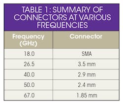
Standard RF cables are prone to damage due to bending, which also causes reflections in the circuit. Bending, bumping, or flexing of a DUT connected to the input of the instrument causes strain on the cable’s input connector and the mounting hardware. Selection of the connector is also an important consideration in a test setup and, as seen in Table 1, is chosen based on the required frequency of operations.
The overall loss of a test cable assembly can be written as:
Loss (dB) = {[Cable attenuation (dB)/100 ft.]/1200}
× (Linches + connector loss) (4)
PCBs for RF/microwave circuits typically involve microstrip, coplanar waveguide (CPW), and stripline circuit configurations. These circuit structures are often used in multilayer PCB designs, and each has its own set of capabilities and limitations. An RF PCB can be fabricated with FR-4 substrate materials having glass fiber and copper in layers bonded by epoxy resins. The main features are high resistance to mechanical stress, good resistance to thermal shock, lightweight but suitable for circuit functions < 2 GHz due to low associated power loss, and interferences.4
PCB routing is divided into two phases: global and detailed routing. Global routing involves the study of optimal component placements, whereas detailed routing is about tracing components between other components. The main design aspects involve avoiding routing near splits and placement of viaholes to avoid disruption of any signal in its return path as a viahole couples it to the plane and causes excitation of parallel-plate modes. Also, an important design step is identification of potential radiators in the circuit and incorporation of preventive methodologies in the design and layout stages, such as a control impedance technique.
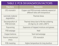
Various analyses such as circuit resonances, emission and enclosure effects must be taken into account separate from any techniques meant to minimize distortion, crosstalk, and ground bounce to ensure clean signal transmission and minimal radiation from the PCB. Higher power handling can be provided by employing a heat sink, thermal vias, and stitching to avoid EMI. Table 2 shows the common causes5 and reasons associated with PCB problems.
Making Measurements
The essential instruments needed for RF//microwave measurements include network analyzers, signal/spectrum analyzers, power meters, oscilloscopes, and signal generators. Of course, unintentional spurious signals can occur inside any of these instruments and propagate through a test system and ultimately be read as a measurement.
RF/microwave test equipment is also prone to the damage caused by improper grounding and handling due to the buildup of electrostatic charge. In case of an extension cable or power cable, a protective ground conductor should be employed for any measurement. For safety, the ground resistance should be checked (<1 Ω) and the voltage between the neutral and ground line should be < 1 V.
A multimeter is one of the fundamental pieces of equipment for measuring ac/dc currents and voltages, resistances, and even temperatures and harmonic frequencies using integrated probes. When choosing a multimeter, main considerations are range, accuracy, and resolution. The accuracy depends on resolution; an improvement in resolution is associated with the measurement range.6 The range selected includes peak hold, min/max for capture of lowest and highest readings, and auto hold/data hold. Safety is a key consideration, too, and various safety features such as voltage arrestors, spark gap, and fuse protection should be incorporated in every unit.
The network and spectrum analyzers differ in the type of signals they explore. A network analyzer is suited for finding signal gain compression and AM/PM conversion, while a spectrum analyzer reads harmonics and makes intermodulation-distortion (IMD) measurements. The network analyzer is equipped with a dedicated source and receiver for displaying ratioed amplitude and phase, while the spectrum analyzer is a sensitive receiver for measuring signal levels, sidebands, harmonics, and demodulated signals.
The main parameters for both the signal generator and network analyzer are frequency range, frequency resolution, spectral purity, output power, and crosstalk. In the case of the spectrum analyzer, it’s a matter of how wide a frequency span it can measure and with what resolution bandwidth (RBW). Spectrum analyzers include selectable input attenuation for choosing which signals to view within a given bandwidth. Various other parameters, such as averaging techniques and amplitude flatness, are selected based on the consideration of measurement accuracy, along with spurious measurements, which in turn affects the measurement speed. Verification of various equipment parameters like spurious-free dynamic range (SFDR), displayed average noise level (DANL), and residual responses is important for freezing the equipment setting at a given time, since an improper setting may incur spurs in the measurement system.
Equipment Calibration
Equipment calibration plays an important part in the overall measurement repeatability of RF/microwave test equipment. Measurements at extremely low levels present challenges to a wide range of test equipment due to the drift and aging of the equipment and other equipment factors.7 Proper calibration practices can help to remove uncertainty errors associated with aging test equipment or to environmental changes. The important aspects in the calibration are traceability and uncertainty. The test calibration of the specific equipment is carried out as per this methodology:
- Signal-generator calibration: The signal-generator output level at assigned frequency is checked with the power meter, and the output level linearity is checked with a power meter and spectrum analyzer. The spectral purity of the signal-generator output is checked for the assigned frequency range with the tunable analyzer.
- Spectrum-analyzer calibration: The spectrum analyzer is initially calibrated with the internal source and then calibrated with the calibrated signal generator for the assigned frequency range.
- Power-supply calibration: The power supply is calibrated for the operating voltage using a calibrated multimeter. Also, the performance of any overvoltage protection is verified using the multimeter. Current limiting is done for the assigned voltage and current and checked with the multimeter.
- Multimeter calibration: The multimeter is calibrated for the operating voltage range using a calibrated power supply.
- Calibration of RF cables: The RF cables used for testing are calibrated for their insertion loss and return loss with a calibrated RF signal generator, spectrum analyzer, and a reference cable.
- Coaxial dc-block calibration: The coaxial dc block is calibrated for its insertion loss with a calibrated RF signal generator, spectrum analyzer, and a reference cable.
The main techniques for calibration are the though-reflect-line (TRL), short-open-load-through (SOLT), open-short-load (OSL), and line-reflect-match (LRM) methods.8,9 Nonlinear distortion measurements like intermodulation and third-order intercept (TOI) with standard stimulus such as two-tone and multitone sources are used, but with complex stimuli, e.g., digitally modulated carriers needed for measurements such as error vector magnitude (EVM) and adjacent channel power ratio (ACPR) measurements. The measurement error modeling can be categorized as systematic errors, random errors, and drift errors. Proper calibration techniques will help minimize these errors.
Measurement errors can lead to system failures and delay a production schedule. The diagnosis of the fault may be aggravated with the temperature cycling associated with the component or workmanship. Improper selection of the component, placement, and attachment can attribute to performance deviation. The same can be corroborated with the measurement equipment by carefully monitoring the performance of each parameter, such as power variation, frequency variation, spurious levels, and noise levels.10
Further integrated package tuning is required to quench oscillations due to parasitic circuit elements. Improper component values, tolerances, voltage rating, and series and parallel resonance frequencies can lead to fluctuations in measurement results. Understanding variations in component values with temperature can best be achieved by a test temperature sequence of ambient, cold, hot, and once again ambient temperatures.
Microwave Case Study
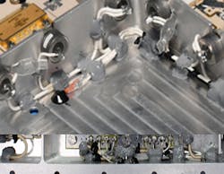
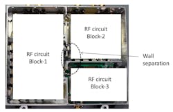
A case study of a microwave transmitter was performed to correlate the various aspects linked with the measurements. A single transmitter assembly consists of multiple cards integrated together in a mechanical box with components for active and passive devices (Fig. 2). Testing of each individual card was meant to be performed and optimized for the intended applications.
2. Spacing and separation of RF/microwave circuits within the packaged portions of a high-frequency test system can avoid problems of interference from re-radiated signals.
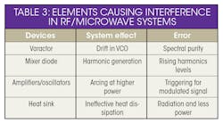
Further integration and assembly is performed after taking into consideration various loadings and parasitics at the desired frequencies.11 The main concern in the transponder is related with the off-band emissions, which can lead to triggering and disrupting the tracking function of the system (Table 3).
Other parameters, such as capacitor polarity, transistor mounting, and diode connections and handling, are important considerations in the overall performance of the system. Testing of the individual transmitter cards along with the package is intended to be carried out in various temperatures and vacuum conditions as encountered by the onboard package under actual operating conditions. The testing sequence of the microwave transmitter case study is as follows:
- Tightening of all connectors and adapters.
- Checking and accounting the losses of the components (e.g., couplers, attenuators) in the test setup.
- Connectors and cables to be mated properly
- Minimizing the bending of the cables.
- Setting the current limit in the power supply.
- Limiting the number of connections and disconnections.
- Prior to the connections, damage or wear such as dirt, nicks to be checked.
- Powering on the system through external console having in-built safety measures.
- Equipment setting to be adjusted as per the specifications and applications.
- Keeping intact the same equipment setting until the end of the package testing.
Current variations in the respective card or package indicate the degradation or shortening effects. Proper diagnosis involves discovering if the degraded device is part of an IC. The analysis sequence requires separation of the active and passive circuitry in the system and probing the pads to correlate the anomaly. In addition, the RF circuits placed in the package must be segregated to avoid the interference effect as shown in Fig. 2. This also helps in the effective grounding of the unwanted signals and further helps in routing of the cables along the walls. Separating susceptible and sensitive cards12 in the package using separation walls, in conjunction with optimized individual circuit performance, results in avoidance of interference effects.
Any cover plate plays an important role due to the radiation phenomena inherently associated with RF/microwave circuits. The radiation-absorbing material at the appropriate locations of the cover plate minimizes the radiation effect. Any loose connections of either the cable or screw at that point leads to fluctuations due to the effect of radiated sources.
For any high-frequency circuit, RF initialization requires that certain precautionary measures be taken to ensure system integrity and accuracy. For example, the power level should be gradually increased to a desired level with continuous monitoring of the output port. For active device card testing, dc should be applied before RF power is applied.
All losses associated with couplers, attenuators, and other passive components should considered, particularly high-power devices that will operate in a shielded area. A loss of 0.5 dB in a 100-W system leads to a power loss of 10 W, so tightening all connectors and adapters should be carried out before beginning any testing.
Steps to be taken prior to powering up the system include:
- Grounding of all metal parts and terminals so that they have common potential.
- Reading the warning labels and not to exceed the values provided.
- Ensuring that body resistance is minimal.
- Tightening of all connectors and adapters.
- Proper routing of cable and wire inside the package.
- Avoiding sharp edges and avoiding nonlinear materials that generate passive intermodulation (PIM), such as copper and nickel.
Apart from the general precautions, other important aspects to consider include the environment, which should be properly ventilated and have humidity control, routing of PCBs to avoid any 90° twist, the power turning on/off sequence, segregation of nonlinear and sensitive PCBs, and the encasing aspects of ESD-prone devices that can minimize the testing-related failures. RF equipment, which is properly supported with a dc block, limiter, or external attenuator, helps to avoid failures related to over-powering. In contrast, improper handling and avoidance of safety precautions can lead to equipment damage and personal injury.13
There’s growing need for testing equipment and test methodologies that can help speed mass market adoption. The choice of equipment and the test plan relates directly with the cost, productivity, cycle time, and throughput of the system. Aging and drift associated with the test equipment impact the system’s overall measurement repeatability. The equipment employed for testing must be properly calibrated along with proper connectors and low-loss cables. By doing so, testing can ultimately be simplified and become more accurate.
References
- David M. Pozar, Microwave Engineering, Wiley, New York, 1989, 3rd ed.
- T. Pearson and M. Madheswaran, “Structural Analysis of High Frequency Parameters for Discrete Components,” International Journal of Computer and Electrical Engineering, Vol. 1, No. 5, December 2009, pp. 1793-8163.
- B. Chakravarti and S. R. Ramasamy, “Practical EMI Guidelines to Microwave Engineers, APMC Proceedings, 1996, pp. 1601-1604.
- Maurizo D. P. Emilo, “High-speed signal layout,” Electronics World, December 2014, pp. 40-41.
- V. Lakshminarayana and N. Sriram, “Case study of failure in PCBs due to thermal stress,” Electronics World, December 2014, pp. 20-23.
- R. Narayanan, “Digital Multimeters: Choose the one with a high impedance,” EFY, October 2001, pp. 31-36.
- Thomas Laverghetta, Practical Microwaves, Prentice-Hall, Englewood Cliffs, NJ, 1996.
- Ananajan Basu, An Introduction to Microwave Measurement, CRC Press, Cleveland, OH, 2015.
- A. J. Estin, J. R. Juroshek, R. B. Marks, F. R. Clague, and J. Wayde Allen, Basic RF and Microwave Measurement: A Review of Selected Programs, Metrological, 1992, pp. 135-151.
- Richard F. Powell, Testing Active and Passive Electronic Components, Marcel Dekker, New York, 1987.
- Keysight Industries, Application Notes, www.keysight.com
- Z. Chen and L. Sun, “Application of test and measurement in microwave device characterization,” 2005 Asia-Pacific Conference Proceedings.
- N. Kupp, H. Huang, P. Drineas, and Y. Marks, “Post production performance calibration in analog/RF devices,” International Test Conference, paper 8.3, pp 1-10, 2010.
