The Wheatstone Bridge: How Does It Impact VNA Measurements?
Download this article in PDF format.
A very wise engineer once told me, “If you want to make an accurate measurement of something, use a bridge.” I have found this advice to be true on more than one occasion. A bridge can be made in many different ways, as long as two paths are conjured up to make a comparison: a reference path and a measurement path.
Here, I’ll only consider the Wheatstone bridge with resistive elements. How might it be used to measure an unknown resistance or complex impedance, or to measure the forward and reverse components of a “traveling wave” over a broad range of frequencies? This last capability is an essential part of a vector network analyzer (VNA), a tool used to determine the S-parameters of a device under test (DUT) by measuring the reflected and transmitted components of incident RF waves in a 50-Ω system.
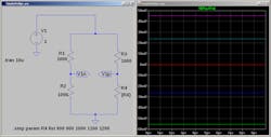
Figure 1 shows a Wheatstone bridge driven by a 1-V DC battery. Resistors R1, R2, and R3 are each 1,000 Ω. R4 takes on the values of 800, 900, 1,000, 1,100, and 1,200 Ω. The plot to the right of the schematic shows the voltage difference between the two arms of the bridge going from −55 to +45 mV, with a 0-V balance occurring when R4 is 1,000 Ω. This makes sense of course. When R4 is 1,000 Ω, the voltage between the resistors of each arm is half of the supply voltage and the difference between them is zero.
1. This figure depicts a Wheatstone bridge circuit. The plot reveals the voltage difference between the two bridge arms.
It’s important to note that at the balance point, small changes and noise from the power supply are canceled out. This is a very important feature. Modern resistance-measurement gear relies on precision voltage references to accomplish this task. However, it’s not required for a bridge.
Circuits like this were used at one time to make precision resistance measurements, primarily in the case of telephone cables. R3 was replaced with a decade box, which could “dial in” a known and precise resistance. The unknown resistance was attached to the R4 position and a sensitive microammeter was placed across the bridge. R3 was then dialed in until the meter read zero volts; the value of R4 must then equal R3.
Directional Bridge, Incident Waves
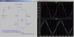
The method described was how resistance was measured with great precision in the past. Now, let’s look at a bridge used to monitor the output of an RF source in a directional manner. We may have a source with a 50-Ω impedance that requires an output-level control. If we have no control over the loading of that source, we will probably want our output-level detector to only look at the incident signal. While a directional coupler will do this over a narrow frequency range, a resistive bridge will operate over a large range—and will probably be less expensive. Figure 2 shows a bridge designed for a directional measurement.
2. Shown is a resistive bridge intended for directional measurements.
The bridge in Figure 2 is balanced due to the resistor values having the same ratio. The ratio of R2 to R1 is 9:1, as is the ratio of the nominal 50-Ω load to R3. This results in a 20-dB coupling ratio and less loss through the RF output path (about 1 dB).
The top chart in Figure 2 (right) shows the current through R1, which would result in a 100-mV peak sine wave across it (2 mA * 50 Ω). The bottom chart shows how the voltage, Vin, varies with the combination of the 50-Ω, 1-V incident wave and reflections caused by loads ranging from 30 to 70 Ω. With a 50-Ω load, there’s no reflection and the red trace shows the 1-V wave with no interference from either constructive or destructive interference.
When setting the load impedance to other values, Vin is either bigger or smaller. This simulation shows how a monitor across R1 would provide a good measurement of the incident wave from the source regardless of loading. Because of the distribution of grounds in this diagram, a balun would be needed across R1, or in place of R1, to “couple off” the signal to a detector, mixer, or other circuit. As long as the “arm” where R1 resides looks like 50 Ω, the bridge will function properly.
Mathematically, if a 10-to-1 or 20-dB sampling of the incident wave is desired, then R1 is set to the source resistance (R6 in Figure 2). The ratio of R2 to R1 and nominal RL to R3 would be 9 to 1, as one would calculate for any other 10-to-1 resistive voltage divider (shown in Figure 2). This example is for a 50-Ω system with a 50-Ω source. For a 75-Ω system, one would simply scale up the resistors accordingly.
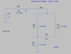
3. In this circuit, the load is replaced with an open circuit.
How does this work? Figure 3 shows the open-circuit condition of the load resistor. A 1-V battery functions as the source. The bridge is 50 Ω in each position to make it easier to see what is happening. In the open-circuit case, the source is seeing 133.333 Ω and the total current is 7.5 mA. That current splits, leaving two-thirds, or 5 mA, across the sense resistor, R1.
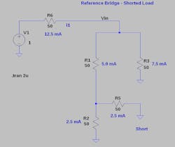
Figure 4 shows the short-circuit case in which the source sees 80 Ω and the total current increases to 12.5 mA. The current splits between R1 and R3, resulting in 5 mA across R1 once again. Therefore, the total impedance seen by the source changes as the load varies from open to short. However, the balancing of the bridge keeps the current through R1 constant in all cases.
4. Here, a short circuit takes the place of the load resistor.
Reflected Waves
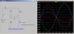
Reflected waves can be measured with a bridge as well. In Figure 5, the load varies from 30 to 80 Ω. The current through R5 is proportional to the reflection from this load. The green and blue curves in the plot represent 30 and 40 Ω. The reflections are anti-phase to the driving waveform. The red trace shows zero reflection at 50 Ω, while the cyan, violet, and gray traces are in-phase reflections with load-resistance values of 60, 70, and 80 Ω.
5. In this analysis, reflected waves are measured with different load-resistance values.
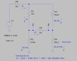
But how does this work? First, let’s substitute source resistor (Rs) values along with K * Rs and Rs/K for a general case. If Rs = 50 and K = 9, we would have the configurations previously shown for a 50-Ω, 20-dB sampling bridge (Figure 6).
6. The last term in the equation shown represents the reflection coefficient.
Taking V1, Rs, and K to be constants, we set up the three equations:
V1 = (i1 * Rs) + (i2 * Rs) + ((i1 − i3) * Rs * K) (1)
V1 = (i1 * Rs) + (i2 * Rs) + (i3 * Rs) + ((i1 − i2 + i3) * RL) (2)
V1 = (i1 * Rs) + ((i1 − i2) * Rs/K) + ((i1 − i2 + i3) * RL) (3)
One can solve for i3 as a function of RL, which turns out to be:
i3 = −V1/2 * (K/(K + 1)2) * 1/Rs * ((RL − Rs)/(RL + Rs)) (4)
Multiplying i3 by the resistor it passes through will give the sampled voltage (V3). The 1/Rs term vanishes:
V3 = −V1/2 * (K/(K + 1)2) * ((RL − Rs)/(RL + Rs)) (5)
V3 = −V1/2 * (K/(K + 1)2) * Γ (6)
Immediately recognizable is the last term in Eq. 5, which is the reflection coefficient of RL with respect to Rs, usually designated by a capital gamma (Γ). We see the not-so-surprising result that the voltage across the middle arm of the bridge provides a simple way to measure the reflection coefficient of any load RL.
In practical terms, it would be necessary to use an instrumentation amplifier or a balun to process this voltage. Many mixers and detectors require a differential input anyway, so this isn’t terribly burdensome.
A VNA might use a combination of source-monitoring and reflection-measuring bridges to provide a very wideband solution. These resistive bridges will essentially operate down to DC and as high as spurious effects allow, which can be very high for a carefully designed bridge with 0201-sized resistors.
In contrast, directional couplers have been used to separate the forward and reverse components of a signal, but they will have a lower cutoff frequency and may operate only over an octave or two of bandwidth. The Wheatstone bridge is a tool that should be in every RF engineer’s toolbox, and in many cases, it might be the ideal solution for a measurement circuit.
The figures and charts for this article were created using LTSpice, a free program available from Analog Devices (ADI). Many thanks to ADI for this great tool.
Brian Walker is Senior RF Design Engineer at Copper Mountain Technologies.
Reference
Dunsmore, Joel. “Simple SMT Bridge Circuit Mimics Ultra-Broadband Coupler,” RF Design, November 1991: 105-108.
