Balanced UHF LNA Simplifies Cell Towers
This file type includes high resolution graphics and schematics when applicable.
Achieving target performance goals in a cellular-communications network can be challenging because of different tradeoffs. For example, the noncoincidence of noise (Γopt) matching and conjugate S11 * impedance matching requires a tradeoff between input matching and amplifier noise figure. Unfortunately, this tradeoff may not be available in cellular infrastructure equipment such as tower-mounted amplifiers (TMAs) because of aerial matching requirements. For example, to achieve a 14-dB aerial mismatch when a low-noise amplifier (LNA) is preceded by a bandpass filter with 18-dB return loss (assumed to be lossless), the input return loss (IRL) must be better than 23 dB. An isolator can alleviate the high reflectivity in a noise-matched amplifier, but it adds cost, size, and loss.
Related Articles
• Tracking Trends in Wireless Infrastructure
• Wireless Technologies Extend Far And Wide
• Cellular Networks Get Primed For Tomorrow
The balanced amplifier topology developed at Bell Labs in the 1960s1,2 is an effective solution because it channels the energies reflected from a pair of amplifiers to quadrature 3-dB couplers (also known as 90-deg. or hybrid couplers) where self-cancellation can take place. Since the port match will be good regardless of the amplifiers’ actual reflectivity, they can be tuned for minimum noise. Additionally, the balanced configuration has better linearity and bandwidth than its single-ended counterpartand is inherently self-stabilizing; high in-band and out-of-band stability is possible even with two potentially unstable amplifiers.3
Of course, a balanced LNA has a higher parts count and power consumption than a single-ended model. Its quadrature couplers also add cost and printed-circuit-board (PCB) area, and their insertion losses degrade noise performances. If commercial drop-in couplers are used, their RF performances are generally proportional to their size. Furthermore, the confined space atop cellular towers does not favor balanced LNAs because they tend to be larger and heavier than their single-ended counterparts. Previous approaches to reducing balanced LNA size involved shrinking the couplers4,5 and higher circuit integration.6,7 However, a TMA’s needs for high sensitivity and linearity tend to hamper miniaturization.
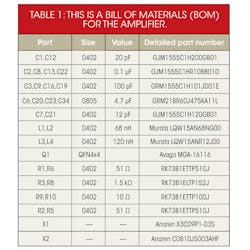
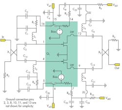
In pursuit of reduced component count and miniaturization in a balanced 900-MHz LNA, a design was developed with miniature multilayer couplers and a MMIC with integrated dual amplifiers, biasing, and shutdown functions. This may be the first time that this type of shutdown function has been integrated in a dual-amplifier MMIC. What follows will describe the materials and methods used to realize the design (Table 1). The first step in reducing the size of a baanced LNA for UHF cell towers involved the design of a new monolithic microwave integrated circuit (MMIC) that integrates dual amplifiers, electrostatic-discharge (ESD) protection, active bias circuitry, and shutdown functions (Fig. 1).

In addition to reducing the number of required external components, this MMIC combines bias circuitry and the amplifier on the same chip, with the benefit of stablizing the operating current against gate threshold voltage and temperature variations. The chip is fabricated with a 0.25-μm enhancement-mode, pseudomorphic high-electron-mobility-transistor (ePHEMT) process on a 6-in. wafer. The process offers a suitable balance of cost and performance.
The process has been proven previously through the fabrication of a single-ended LNA capable of 0.3-dB noise figure at 900 MHz,8 making it appear that a 0.5-dB noise figure in balanced mode might be possible after factoring in the coupler’s loss. The process’s high transition frequency (fT) of greater than 30 GHz and high peak transconductance of about 615 mS/mm make it possible to reduce the number of gain stages to just one to reach a gain level of 17.6 dB. In addition, the process is suitable for low-voltage operation because its linearity does not degrade appreciably until the drain-source voltage, VDS, falls below 2 V.9 The MMIC, which integrates 6 transistors, 26 diodes, 12 resistors, and 2 capacitors, is epoxy encapsulated in a 16-pin 4 x 4 x 0.85 mm quad flat no-lead (QFN) package.
The active bias circuits are connected to the voltage supplies Vdd1-2 via external resistors R3 and R8. Through these resistors, the gate bias voltages can be controlled by the user. Although each ePHEMT’s nominal drain current, Idd, is 60 mA at a drain voltage, Vdd, of +4.8 VDC, it can be varied from 48 to 72 mA over the usable range of values for these resistors. Inductors L1 and L16 and resistors R1 and R6 serve as the gates’ (pins 1 and 4) bias networks. Although on-chip spiral inductors can perform this function, this design employs external inductors because they have lower losses, the smaller chip is more economical, and the chip can be used at other frequencies.
Ampilifer Assembly
Since noise figure is critical in this application, wirewound chip inductors were used instead of multilayer inductors. Beside bias insertion, the aforementioned inductors and series capacitors, C3 and C16, also form high-pass networks to roll off unneeded low frequency gain. The long bondwires, Lw, which connect the drain to the package leads also serve as prematching structures.
The shutdown function block consists of transistor switch in series with the active bias. Shutdown is initiated by applying a high logic (≥ 2 V) at Vsd1/2 to open the switch. Conversely, a low logic ( i.e., Vsd1/2 ≤ 500 mV), turns on the amplifiers. Transitioning from normal to shutdown mode takes less than 50 ns if the large (≥ 0.1 μF) decoupling capacitors C6, C8, C20, C22, C23, and C24 are omitted. However, these capacitors are generally recommended because they aid low-frequency stability and dampen supply transients.
This file type includes high resolution graphics and schematics when applicable.
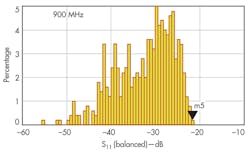
Although a Lange coupler is the most compact type of coupler component, its extremely fine trace width is not suitable for PCB implementation. As a result, the balanced LNA design uses commercially available multilayer couplers, X1-2, to perform signal combining and splitting. A larger coupler measuring 6.4 x 5.1 mm is used at the input because of its lower loss, while a smaller coupler measuring 2.0 x 1.3 mm is used at the output to save space and cost. To ensure that the input return-loss requirement of 21 dB or better can be met without fail in volume production, the critical parameters were identified through a Monte Carlo analysis. Subsequently, two controls were instituted: correlating the amplifiers’ input match to |S11a - S11b| < 0.025 and ensuring that the input coupler’s isolation is greater than 23 dB. The first control was satisfied by using adjacent chips, while the second required specifying a high-isolation input coupler.10 The output coupler is not critical. As a result, the worst-case input return loss measured in 500 samples was 21.5 dB (Fig. 2).
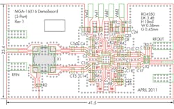
The PCB for the balanced LNA is built on RO4350 circuit-board material (Fig. 3) from Rogers Corp. Wherever practical, microstrip linewidths were dimensioned for a characteristic impedance of 50 Ω. However, circuit traces next to the input coupler’s mounting pads are necked down following the manufacturer’s recommendations to compensate for the pads’ parasitic capacitances. An FR-4 circuit-board layer was added to the 10-mil-thick PCB to increase the stack height to 1.6 mm. The input and output microstrip lines are transitioned to coaxial connectors using edge-launched SMA receptacles. All performance results are referenced to the coaxial ends.
Put To The Test
Circuit simulations were performed with ADS2009 Advanced Design System (ADS) software from Agilent Technologies, with the circuit model split into a two-level hierarchy (Fig. 4). The upper level consists of blocks representing the MMIC, the signal dividing/combining circuitry, and the impedance-matching functions. Each dual amplifier, Q1 and Q2, is represented by identical two-port S-parameter (.s2p) files. The S-parameters were previously extracted on a test fixture of similar material (10-mil-thick RO4350 circuit-board material) and then applying a through-reflect-line (TRL) calibration to shift the reference planes to the package edges.
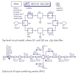
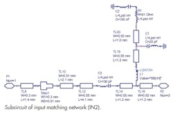
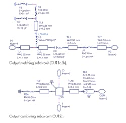
With the same test fixture, the device’s noise and linearity parameters were extracted using automated source and load-pull tuners from Focus Microwaves. The ~0.2-dB NFMIN value is particularly challenging to extract because it can be easily obscured by the combined losses of the mechanical tuner and the required APC7-to-3.5-mm coaxial connector adapter. The inductors and hybrid couplers are modeled with their manufacturers’ .s2p data. Other passive components are modeled using their equivalent-circuit models, including their lower-order parasitic values.
This file type includes high resolution graphics and schematics when applicable.
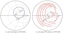
To validate the designed input and output matching networks, the modeled source impedance, ΓS, and load impedance, ΓL were compared with previously measured source- and load-pull contours. The ΓS and ΓL modeled values were obtained via simulation with the ADS “S-parameter probe” component. The balanced LNA MMIC makes it easy to achieve good noise performance because the 0.3-dB constant NF circle is large and even encompasses the chart center (Fig. 5, left). Because of this, the input networks comprising L1 - C3 and L2 - C16 are designed to function as bias tees rather than as impedance/noise matching networks.
Conclusions
The absence of impedance tranformations in the input LC network means that the bandwidth is not constricted by the network’s loaded quality factor (Q) and the insertion loss is less sensitive to component Q. The value of ΓS offset from the chart center is unintentional and is due to the parasitic elements of the lumped components; the noise figure associated with ΓS is 0.28 dB. Any optimization of the noise match Γopt will prove to be insignificant, providing at most an improvement of 0.03 dB and not justifying the effort of performing the optimization.
The balanced LNA circuit has an output third-order intercept point (OIP3) of better than +42 dBm at optimum output match. The area encompassed by the +42-dBm constant linearity circle will require some impedance transformation since it is located away from the center of the chart (Fig. 5, right). The next lower constant linearity circle, at +40 dBm, includes the chart center. Since a +40-dBm OIP3 is adequate for this application, the output network was designed without impedance transformation (i.e., ΓL = 50 Ω). However, ΓL is shown slightly offset from the exact center becauseof component parasitic elements.
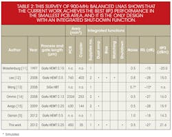
The LNA’s PCB area is 40% smaller than the nearest competitor (Table 2). Moreover, its single-voltage supply requires fewer components to implement than most amplifier solutions for this application. To the author’s knowledge, this is the first dual-amplifier MMIC that integrates a shutdown function. Its noise figure is as good as competing designs using larger couplers and more expensive, shorter-gate-length semiconductor processes (Table 2).11-15 The amplifier’s experimental noise figure and gain are 0.5 dB and 18 dB, respectively, at 900 MHz (Fig. 6).
The circuit model developed for this design has good predictive value because the maximum errors for noise figure and gain are 0.1 and 0.2 dB, respectively, over a 1-GHz range. If not for losses from the input coupler and matching network, the balanced LNA’s noise figure would have been equal to its constituent amplifiers.16 Since the individual amplifiers’ noise figures are about 0.3 dB, it is assumed that the combined loss of the input coaxial connector and hybrid coupler is about 0.2 dB. This design can potentially serve multiple wireless communications standards (e.g., GSM and LTE) because its noise figure changes less than 0.1 dB from 600 to 1050 MHz. The noise figure increases abruptly outside this frequency range due to the input coupler’s characteristics.
This file type includes high resolution graphics and schematics when applicable.
Summing Up
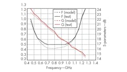
The experimental result surpasses the -21-dB input mismatch required by TMAs. Morever, the good impedance matching is maintained over a wide bandwidth; i.e., equal to 83% of the center frequency (fc) at IRL ≤ -20 dB (Fig. 7). The experimental IRL is best around the input coupler’s center frequency. Likewise, the output coupler determines the output-return-loss (ORL) response. The model has semiquantitive agreement with the experimental result over most of the passband. However, the experimental ORL’s unexpected dip at 500 MHz was not predicted by the model, and this could be due to failure to model a component’s parasitics. As previously mentioned, the quadrature couplers enable the extremely wide matched bandwidth. Both input and output return loss are limited by the couplers’ finite isolation and by the microstrip discontinuities.

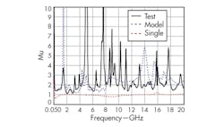
The balanced LNA is unconditionally stable even when its constituent amplifiers are not. Both modeled and measured μ stability factor exceed unity over 50 MHz to 20 GHz (Fig. 8). Therefore, the balanced topology’s self-stabilizing promise is validated because the individual amplifiers are potentially unstable (μ < 1) at several frequencies over the evaluated range. The calculated stability factor has the same general trend as the experimental result, but their peaks do not converge exactly because of the grossly simplified passive component models.
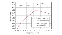

The author notes that the input third-order intercept point, IIP3, is the highest ever reported (Table 2). The output power at 1-dB gain compression (P1dB) measures about +24 dBm at midband and is relatively constant over frequency, varying less than a 1 dB over a 1-GHz span (Fig. 9). The IIP3 was measured using -20-dBm input signals spaced 1 MHz apart, reaching +21.6 dBm at midband, or about 5 dB better than a competitive solution. But unlike the flat P1dB response, the IIP3 exhibits a pronounced peak (+21.9 dBm) at the approximate center of the couplers’ passband. Referred to the output, the OIP3 is about +39.6 dBm at midband. The linearity figure of merit based on the ratio of OIP3 to DC power is about 15.7. In the noisy RF environment of a shared antenna tower, this design’s high P1dB and IIP3 values will support immunity to blocking and spurious mixing, respectively.
Activating the MMIC’s shutdown function transforms the amplifier into a nonreflective attenuator which can be used to prevent the overloading of subsequent stages. Signals passing through the shutdown amplifier are attenuated by about 16 dB at midband, while the input and output return losses are better than 20 dB (Fig. 10). Good impedance matching is maintained during shutdown because reflected energies are self-cancelled in the couplers. In comparison, an unpowered single-ended amplifier is highly reflective and must be bypassed when shutdown to prevent detuning of aerial and filter. To the author’s knowledge, this is the first time this desirable LNA property has been reported and proposed for eliminating the customary LNA bypass switch in cellular towers. The current consumption for the balanced amplifier is a negligible ~176 μA per channel during shutdown.
In conclusion, balanced 900-MHz LNAs can be made more compact by designing around a MMIC with multiple integrated functions. The MMIC’s good noise performance allows smaller but lossier couplers to save space. The TMA’s low impedance mismatch requirements can be met by controlling differences between the amplifier’s S11 performance and the coupler’s isolation. The excellent impedance matching achieved during the LNA’s shutdown mode offers the potential to eliminate the need for LNA bypassing in cellular towers. This new design should enable smaller and better performing tower-mounted balanced LNAs.
Chin-Leong Lim, Engineer
Avago Technologies, 11900 Bayan Lepas, Penang, Malaysia; (604) 610-2525.
Acknowledgments
The author would like to thank Zulfa for the technical discussion, M.D. Suhaiza and S. Punithevati for fabricating the prototype, S.A. Asrul for reviewing the draft, and the management of Avago Technologies for approving the publication of this work. Anaren Communications (Suzhou) provided the couplers at no charge.
This file type includes high resolution graphics and schematics when applicable.
References
1. M. Eisele, R.S. Engelbrecht, and K. Kurokawa, “Balanced Transistor Amplifiers for Precise Wideband Microwave Applications,” IEEE International Solid-State Circuits Conference, February 1965.
2. R.S. Engelbrecht and K. Kurokawa, “A Wideband Low Noise L-Band Balanced Transistor Amplifier,” Proceedings of the IEEE, Vol. 53, No. 3, March 1965, pp. 237-247.
3. S.C. Cripps, RF Power Amplifiers for Wireless Communications, Artech House, Norwood, MA, 1999, Section. 10.2: “Balanced amplifiers.”
4. J.S. Mandeep and H. Abdullah, “A compact, balanced low noise amplifier for WIMAX base station applications,” Microwave Journal, November 2010.
5. A.F. Osman and N. Mohd. Noh, “A design for SDR radio using balanced amplifier topology,” 4th Asia Symposium on Quality Electronic Design, 2012.
6. T. Chong, “A Low-Noise, High-Linearity Balanced Amplifier in Enhancement-mode GaAs pHEMT Technology for Wireless Base-Stations,” Proceedings of the European Microwave Conference, Paris, France, October 2005.
7. T. Chong and S. Rendava, “Design and Performance of a 1.6-2.2GHz Low-Noise, High Gain Dual Amplifier in GaAs E-pHEMT,” Asia-Pacific Microwave Conference, Suzhou, China, December 2005.
8. C.L. Lim, “Setting new noise performance benchmarks using wideband low-noise high-linearity LNAs,” Microwave Journal, February 2011.
9. J. Madden, “Low voltage operation of GaAs power amplifier,” Microwave Journal, September 2006, pp. 130-134.
10. Anaren product specification, “X3C19P1-03S hybrid coupler,” Rev. D.
Related Articles
• Tracking Trends in Wireless Infrastructure
• Wireless Technologies Extend Far And Wide
• Cellular Networks Get Primed For Tomorrow
11. E.E.M. Woestenburg, “LNAs for the multi frequency front ends,” Netherlands Foundation for Research in Astronomy, Dwingeloo, NFRA-ITR 219, December 1997.
12. H.K. Lee, A.C.S. King, H. M. Fuad, and T. Chong, “A low noise figure high linearity balanced amplifier module for cellular band base station’s tower mounted amplifier application using E-mode pHEMT Technology,” Proceedings of the 2008 Asia-Pacific Microwave Conference.
13. Z. Wang, W. Yang, J. Peng, J. Chen, W. Xie, and C. Shi, "The design of SiGe HBT balanced broadband low noise amplifier,” International Conference on Microwave & Millimeter Wave Technology, 2008.
14. Ommic product specification, “CGY2106XHV Dual Ultra Low Noise High IP3 Amplifier."
15. Avago Technologies, application note 5441, “LNA Design with the MGA-16516 Matched Pair, Low Noise Amplifier.”
16. G.V. Petrov, “Noise properties of balanced amplifiers,” International Journal of Electronics, Vol. 53, No. 5, 1982.
This file type includes high resolution graphics and schematics when applicable.
