Current Reuse Gains UWB LNA

This file type includes high resolution graphics and schematics when applicable.
Since the United States’ Federal Communications Commission (FCC) earmarked the spectrum from 3.1 to 10.6 GHz for ultrawideband (UWB) communications use, interest has increased in the development of components for this broad bandwidth. The frequency band holds great promise for high-data-rate wireless communications and is geared to co-exist with licensed wireless applications within the more narrowband segments in that frequency range. Of course, producing high-frequency components capable of operating within the UWB frequency range—such as low-noise amplifiers (LNAs)—is critical to the use of practical UWB applications.
Related Articles
• Compact LNA Drives 2.5-GHz Base Stations
• LNA Boosts 6 To 20 GHz
• Variable-Gain LNA Reaches 26 GHz
Unfortunately, the LNA is one of the greater challenges in terms of UWB components. But with the proper circuit design and semiconductor process, such a broadband low-noise amplifier can be produced with high gain and low noise figure.
Of course, minimizing the power consumption of an LNA for UWB applications is another important requirement. This is no trivial design task, even with the benefit of excellent modern semiconductor processes. UWB LNAs for frequency bands of 3.0 to 5.0 GHz and 3.1 to 10.6 GHz have been widely reported based on silicon CMOS technology.1-6 Another UWB LNA was reported for the frequency band of 2 to 6 GHz, with current reuse topology utilizing a noise-shaping technique.7
The current report highlights a broadband CMOS LNA for UWB applications from 3 to 7 GHz. It employs current-reuse techniques to minimize power consumption and enhance gain at the upper end of the frequency range. A shunt peaking inductor was used to improve flatness gain and to increase the total bandwidth, while a common-drain amplifier helps achieve a wideband output impedance match for measurement purposes.
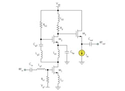
The proposed LNA is a two-stage amplifier with a current-reuse cascade common source structure, useful both for saving power consumption and maintaining good power gain. The two-stage design, initially targeted for power consumption of 6 mW from a +1-VDC supply, is shown in Fig. 1. This results in drain current of approximately 6 mA. Assuming a 6 mA current drawn by transistor M1 for the first stage, the calculated size for transistor M1 is approximately 150 μm based on Eq. 18:
ID ≈ 0.5μnCox(W/L)(VGS1 – Vt)2 (1)
where:
VGS1 = +0.7 VDC;
Vt = +0.5 VDC; and
μnCox = 369 μm for a typical 0.18-μm silicon CMOS semiconductor process.
The required transconductance, gm1, can be determined by Eq. 2:
gm1 = ∂IDD/∂IGS1 = μnCox(W/L) (VGS1 – Vt) (2)
Rearranging Eq. 1 to:
(VGS1 – Vt = [2IDD/μnCox(W/L)]0.5
and substituting into Eq. 2, the equation for gm1 can be simplified to Eq. 3:
gm1 = [2μnCox(W/L)ID]0.5 = (2βID)0.5 (3)
where β = μnCox(W/L) is known as the transconductance parameter. Hence, the calculated gm1 is approximately 60.7 mA/V.
By ignoring the Miller effect of gate-drain capacitance (Cgd1) on transistor M1, the input impedance of M1 can be given by Eq. 49:
Zin1 = jω(Lg1 + Ls1) + (1/jωCgs1 + gm1Ls1/Cgs1 (4)
where:
gm1 = the transconductance of M1;
Cgs1 = the gate-source capacitance of M1;
Ls1 = the source degeneration inductor; and
Lg1 = the gate input inductor.
The real part of the input impedance in Eq. 4 is given by Eq. 5:
ReZin1 = gm1Ls1/Cgs1 (5)
With given values of gm1 and Cgs1, the desired impedance match to Rs (usually 50 Ω) can be obtained by setting Ls1 accordingly. The imaginary part of the input impedance can then be compensated with an input matching inductance, Lg1. The corresponding resonant frequency, ω0, is approximated by Eq. 6:
ω0 ≈ [1/(Ls1 + Lg1)Cgs1]0.5 (6)
The source generation inductor, Ls1, is added for linearity and stability improvement, whereas the gate inductor Lg1 is needed for impedance matching between the source impedance and input of transistor M1. In this design, the value of inductor Ls1 is chosen to be small enough (approximately 0.5 nH) so that it could be easily replaced by a bondwire inductance in order to reduce the chip area when necessary. Next, the value of gate inductor Lg1 is calculated from Eq. 6 to be approximately 1.5 nH using a resonant frequency of 5 GHz.
The current-reuse topology employs transistor M2 stacked on top of the input transistor M1 to save power consumption. The current-reuse function is implemented by Ld1, Lg2 and Cg2 to boost gain. Inductor Lg2 must form a series-resonant circuit with capacitance Cg2 and the input capacitance Cgs2 of transistor M2 to create a low-impedance path to couple the output of M1 to the input of M2, while inductor Ld1 is chosen to be large enough to provide a high-impedance path to block the signal in the desired band.10 Parameter Cbp is a bypass capacitor. Therefore, the input can be amplified twice under this concurrent scheme.
It should be noted that the series resonant circuit consisting of Lg2 and Cg2 exhibits a narrowband characteristic. Consequently, the current-reuse function is maximized around the resonant frequency, which is designed to enhance the gain at the upper end of the desired frequency band.
This file type includes high resolution graphics and schematics when applicable.
Reducing Power Consumption
This file type includes high resolution graphics and schematics when applicable.
To achieve low power consumption, the width of transistor M1 is set to 260 μm, while the width of M2 is set to 200 μm. The inductances of Ld1 and Lg2 are 5.3 and 1.8 nH, respectively. Resistor Rb2 is used to provide bias voltage for transistor M2. The inductor Ld2 (2.3 nH) and resistor Rd (54 Ω) are chosen to provide inductive peaking for extending the frequency range and providing peak gain at the center of the passband, achieving nearly flat overall wideband LNA gain. The last stage of the LNA consists of transistor M3 and the current source is the 50-Ω buffer for measurement purposes. Capacitors Cin and Cout are DC blocks.
The current-reuse amplifier functions as a two-stage cascade amplifier. The noise figure of the second stage contributed by both the MOSFET (device M2) and inductors Lg2 and Ld1 can be reduced by the gain of the first stage. With this design technique, not only is high gain possible, but low noise figure can be achieved simultaneously.
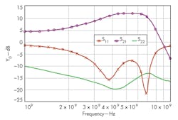
Figures 2 through 6 offer simulation results for the proposed UWB LNA for simulations performed with the SpectreRF simulation program from Cadence Design Systems, utilizing a 0.18-μm silicon CMOS semiconductor process from Taiwan Semiconductor Manufacturing Co. (TSMC). Figure 2 shows the small-signal S-parameters, where it can be seen that the UWB LNA achieves average simulated gain of 10.6 dB from 3 to 7 GHz, with gain flatness of better than 1.5 dB. The maximum gain of 12.3 dB occurs at 5 GHz.
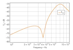
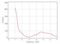
Over the frequency range of interest, the input return loss (S11) is less than 7.7 dB, while the output return loss (S22) is less than 13 dB. The reverse isolation is less than -36 dB from 1 to 10 GHz, as shown in Fig. 3. The stability factor (K-factor) was also computed using S-parameter data and was found to be greater than 1 across the frequency range from 1 to 8 GHz (Fig. 4). This indicates that the proposed LNA is unconditionally stable across the frequency range of interest.
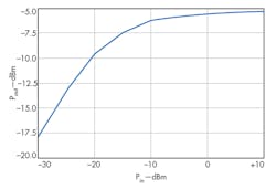
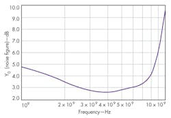
As Fig. 5 shows, the noise figure is better than 3.3 dB between 3 and 7 GHz with minimum noise figure of 2.6 dB at 4.3 GHz. The output power versus input power was measured for a single test tone at 5 GHz (Fig. 6), with a 1-dB compression point of about -10 dBm. The power consumption is only about 7 mW from a +1-VDC supply, which includes the power of the output buffer.
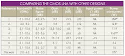
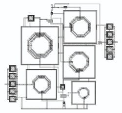
The table summarizes the measured performance of the UWB LNA compared to previous works. The layout is shown in Fig. 7. The amplifier can achieve a wide bandwidth, high gain, and low noise figure while also operating with minimal power consumption—about 7 mW across a frequency range of 3 to 7 GHz.
This file type includes high resolution graphics and schematics when applicable.
References
This file type includes high resolution graphics and schematics when applicable.
1. A. Bevilacqua and A.M. Niknejad, “An Ultra wide band CMOS Low-Noise Amplifier for 3.1-10.6 GHz Wireless Receivers,” IEEE Journal of Solid-State Circuits, Vol. 39, No. 12, 2004, pp. 2259-2268.
2. C.W. Kim, M. S. Kang, P.T. Anh, H.-T. Kim, and S.G. Lee, “An Ultra-Wideband CMOS Low Noise Amplifier for 3-5 GHz UWB System,” IEEE Journal of Solid-State Circuits, Vol. 40, No. 2, 2005, pp. 544-547.
3. Y. Lin and S.H. Hsu, “A 3.1-10.6 GHz Ultra-Wideband CMOS Low Noise Amplifier with current reused technique,” IEEE Microwave and Wireless Components Letters, Vol. 17, No. 3, 2007, pp. 232-234.
4. H.L. Kao, A. Chin, K.C.Chang, and S.P. McAlister, “A low-Power Current-Reuse LNA for Ultra-Wideband Wireless Receivers from 3.1 to 10.6 GHz,” 2007 Topical Meeting on Silicon Monolithic Integrated Circuits in RF Systems, 2007, pp. 257-260
5. Z.Y. Huang, C.C. Huang, Y.T. Hung, and M.P. Chen, “A CMOS Current Reused Low-Noise Amplifier for Ultra-Wideband Wireless Receiver,” ICMMT, 2008, pp. 1499-1502.
Related Articles
• Compact LNA Drives 2.5-GHz Base Stations
• LNA Boosts 6 To 20 GHz
• Variable-Gain LNA Reaches 26 GHz
6. K.T. Ansari and C. Plett, “A CMOS Low Power Ultra-Wideband LNA Utilizing Feedback Technique,” Microsystems and Nanoelectronics Research Conference, 2009, pp. 5-8.
7. W.H. Hung, K.T. Lin, J.Y. Hsieh, and S.S. Lu, “A 2-6 GHz Broadband CMOS Low-Noise Amplifier with Current Reuse Topology Utilizing a Noise-Shaping Technique,” ISCAS, 2011, pp. 1291-1294.
8. B. Razavi, Design of Analog CMOS Integrated Circuits, McGraw-Hill, New York, 2001.
9. T.H. Lee, The Design of CMOS Radio-Frequency Integrated Circuits, 2nd ed., Cambridge University Press, New York, 2004.
10. S.A.Z. Murad, R.K. Pokharel, R. Sapawi, H. Kanaya, and K. Yoshida, “High Efficiency, Good Linearity, and Excellent Phase Linearity of 3.1-4.8 GHz CMOS UWB PA with a Current-Reused Technique,” IEEE Transactions on Consumer Electronics, Vol. 56, No. 3, 2010, pp. 1241-1246.
This file type includes high resolution graphics and schematics when applicable.
