Converters Channel High-Speed Signals
Analog and digital signals are found in many high-frequency systems, which rely on the signal conversion capabilities of analog-to-digital converters (ADCs) and digital-to-analog converters (DACs) to process them. To their credit, suppliers of high-performance ADCs and DACs continue to push the clock speeds and performance levels of their converters, making them compatible with an increasing number of applications around the industry. These range from wired and wireless communications systems to the most advanced test-and-measurement equipment.
Related Articles
• Low-Power Mixer Converts UWB Signals
• Data Converters Drive RF Designs
• Converting Frequencies With Microwave Mixers
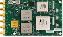
Not-so-ironically, some of the highest-performing data converters are available from the same companies that build test equipment, such as the 8-b TADC-1000 ADC module from Tektronix Component Solutions. The ADC board (Fig. 1) measures 3.6 x 5.9 x 1.5 in. It features an analog bandwidth of better than 8 GHz with sampling rates to 12.5 GSamples/s on one channel and 6.25 GSamples/s per channel on two channels. The digitizer module is designed for use with an external clock. It can work across a range of input clock frequencies from 1.60 to 3.125 GHz, to achieve sample rates from 8.0 to 12.5 GSamples/s in single-channel mode and 4.00 to 6.25 GSamples/s in dual-channel mode.
The TADC-1000 ADC module can stream data continuously at 100 Gb/s and maintain that streaming rate across the full bandwidth. The ADC achieves a high effective number of bits (ENOB) by means of onboard calibration. Built with devices based on the high-speed silicon germanium (SiGe) BiCMOS process from IBM, the firm’s application-specific-integrated-circuit (ASIC) design team interleaves four ADCs operating at 3.125 GSamples/s using advanced clocking techniques for synchronization. It is the same ASIC technology that has been used and proven in a number of the company’s high-performance test instruments. The digitizer module offers a spurious-free dynamic range (SFDR) of better than -47 dBc to 5 GHz with about 15 W power consumption.
Targeting the other side of data conversion, the firm also offers the model TDAC-2000 single-channel DAC, which is capable of operating to 12 GSamples/s. The 10-b DAC module features a single-ended CMOS parallel interface and can stream continuously at rates to 120 GSamples/s. The module consists of multiplexers and a high-speed DAC, with data supplied to the multiplexers via 320 data lines at 375 Mb/s, for the aggregate rate of 120 GSamples/s. The high-speed DAC is well suited for applications in electronic-warfare (EW) systems, radar systems, and in digital radio-frequency memories (DRFMs).
In terms of speed, Fujitsu Microelectronics Europe (FME) has set some data converter marks in recent years, having combined its CHArge-mode Interleaved Sampler technology (CHAIS) with standard 65-nm CMOS semiconductor process technology. The fabrication approach, unveiled in 2009, enabled the integration of multiple ADCs with signal-processing circuitry and memory on a single chip, nominally for high-speed coherent receivers in optical communications systems.
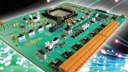
The 65-nm process has fabricated 8-b ADCs with sampling rates to 56 Gsamples/s per channel with only 2 W power consumption per channel, and with a half-speed mode of 28 Gsamples/s with only 1 W power consumption per channel. The converter approach works with a 1.75-GHz input reference clock, using internal multiplication to provide the required internal clock rates with low jitter. Earlier this year, Fujitsu Semiconductor Europe (FSEU) applied its 28-nm CMOS process to the development of low-power, 28-nm 8-b ADCs capable of supporting sampling rates from 55 to 70 GSamples/s with scalable analog bandwidths (Fig. 2).
The Need For Speed
Aiming for speed with somewhat reduced resolution, Hittite Microwave Corp. recently augmented its lines of low-power 8-to-14-b ADCs operating at lower clock rates with numerous high-speed, lower-resolution ADCs capable of running at sampling rates to 26 GSamples/s. These devices leverage the company’s track-and-hold design patents and advanced packaging capabilities in support of wideband receiver and test-equipment designs through Ku-band frequencies, at operating temperatures from -55 to +85°C.
For example, model HMCAD5831LP9BE is an ADC with integral over-ranging, inhibit, and 1:2 demux circuitry that operates at maximum sampling rates to 26 GSamples/s and typical sampling rates to 20 GSamples/s. It offer 3-b typical resolution for a typical Nyquist input bandwidth of 20 GHz and is supplied in a 64-lead plastic RoHS-compliant 9 x 9 mm SMT package. A data-inhibit function makes it possible to set ADC outputs to zero, and output data can be modulated by an external clock using the XOR CML input port. The ADC’s single-ended RF input can be AC or DC coupled and supports broadband operation. The data converter operates on -5- and -3.3-VDC voltage supplies.
Texas Instruments recently announced a number of single- and dual-channel converters with 12-b resolution and low power consumption. For example, model ADS5402 is a dual-channel device with two 12-b 800-MSamples/s ADCs that support a 1.2-GHz 3-dB input bandwidth. The converter operates with power dissipation of just 1.1 W/channel and boasts an SFDR of -74 dBc at 230 MHz for a 1-V peak-to-peak full-scale input. It operates at a maximum clock rate of 800 MSamples/s and is supplied in a 12 x 12 mm, 196-pin BGA package.
The company also offers a single-channel version, model ADS5401, with just 1.33 W/channel power dissipation and the same SFDR of -74 dBc. It boasts performance for one channel that is similar to that provided by the two-channel model ADS5402. Both are designed for the full industrial operating temperature range of -40 to +85°C. The low-power converters are suitable for microwave receivers, radar systems, satellite communications (satcom) systems, signal intelligence (SIGINT) receivers, and software defined radio (SDR) systems.
Analog Devices, which is known for both its ADCs and DACs, supports a wide range of data converters from audio frequencies through microwave frequencies. As an example, model AD9129 is a high-resolution, 14-b DAC that supports data rates to 2.8 GSamples/s. It is based on a quad-switch architecture that enables operation to 5.6 GSamples/s, with 2x interpolation for generation of multicarrier analog signals through 4.2 GHz.
Related Articles
• Low-Power Mixer Converts UWB Signals
• Data Converters Drive RF Designs
• Converting Frequencies With Microwave Mixers
The DAC has been used in cable-television (CATV) applications requiring many contiguous carriers with wide dynamic range. Based on NMOS semiconductor technology and fabricated on a 0.18-μm silicon CMOS process, the converter operates from +1.8 and -1.5 VDC supplies. The output current can be programmed over a range of 9.5 to 34.4 mA. The DAC includes a dual-port, source synchronous LVDS interface and a frame/parity bit is also included to monitor the integrity of the interface. It also features on-chip delay locked loops (DLLs) to optimize the timing between different clock domains. The AD9129 is supplied in a 160-ball chip-scale BGA package.
To aid designers, many data converter suppliers offer reference designs that provide a starting point for interleaving multiple devices and operating at accelerated clock rates. A 12-b, 2-GSamples/s reference design from Intersil, for example, interleaves four of the company’s model ISLA112P50 12-b, 500-Msamples/s ADCs to achieve the ADC board rate of 2 Gsamples/s. This reference design boasts an SNR of 65.5 dB full scale with an input signal of 190 MHz, and a SFDR of -82 dBc for an input signal of 190 MHz. Many other suppliers of data converters, such as Analog Devices, Linear Technology, Maxim Integrated Products, NXP Semiconductors, and STMicroelectronics offer reference designs based on both their ADCs and DACs to help guide designers.
About the Author
Jack Browne
Technical Contributor
Jack Browne, Technical Contributor, has worked in technical publishing for over 30 years. He managed the content and production of three technical journals while at the American Institute of Physics, including Medical Physics and the Journal of Vacuum Science & Technology. He has been a Publisher and Editor for Penton Media, started the firm’s Wireless Symposium & Exhibition trade show in 1993, and currently serves as Technical Contributor for that company's Microwaves & RF magazine. Browne, who holds a BS in Mathematics from City College of New York and BA degrees in English and Philosophy from Fordham University, is a member of the IEEE.

Leaders relevant to this article:


