Interview: Element Six's Adrian Wilson
NF: Element Six is actually a member of the DeBeers Group of Companies, which makes sense considering Element Six’s focus on synthetic diamond supermaterials. How does being a member of a jewelry giant help Element Six serve customers involved with electronics?
Related Articles
• Interview: Blake Peterson, Microwaves & RF “Living Legend”
• Interview: Greg Maury, President, Maury Microwave
• In Memoriam: RLC Electronics’ Founder, Alan Borck
AW: Being owned by DeBeers actually puts us in a very strong position to address the semiconductor market—particularly from a commercial perspective. As you know, the adoption of new materials in the semiconductor industry can take many years. You first need to convince early adopters of the benefits of the material and then be designed in. As a consequence, owners or investors of companies participating in the semiconductor industry must be prepared to invest over a relatively long period of time before the attractive returns on investment are achieved.
One of the commercial benefits of being owned by DeBeers is its familiarity in making long-term investments. As I am sure you can appreciate, the time from starting diamond exploration to having a high-yielding mine can take many years, which is analogous to adoption times in the semiconductor industry.
DeBeers created Element Six over 50 years ago, with microwave synthetic-diamond development investment starting a little over 25 years ago. It is this tenure of investment that has allowed us to provide grades of synthetic diamond that are leading the way in thermal management for semiconductor devices.

NF: Can you explain how Element Six synthesizes diamonds?
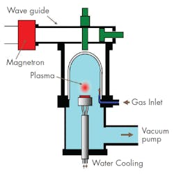
AW: Element Six leverages its proprietary microwave chemical-vapor-deposition (CVD) process to grow synthetic diamonds from a hydrocarbon gas mixture. CVD diamond synthesis generally occurs below atmospheric pressure, typically between 1 and 200 Torr (see figure). Through CVD synthesis, we are able to tightly control growth conditions, eliminate chemical impurities, and engineer various properties into polycrystalline or single-crystal diamond material, depending upon the product specification. This ensures production of a highly consistent material with predictable properties and behavior that enables a diverse range of applications, such as heat spreaders for high-power electronics and in RF optics as exit windows for high-power gyrotrons and beam line windows.
NF: With the acquisition of Group4 Labs—a semiconductor wafer materials company and manufacturer of gallium-nitride-on-diamond (GaN-on-diamond) devices—Element Six has a chance to bring GaN-on-diamond technology into wider use. What technology and capabilities has Element Six gained with this acquisition?
AW: The acquisition of Group4 Labs (G4L) assets and intellectual property earlier this year has expanded Element Six’s semiconductor portfolio to further address defense and additional commercial applications. Specifically, we now have the ability to enable higher-performance GaN devices—resulting in smaller, faster, and higher-power electronic devices in these two market sectors.
Our GaN-on-diamond substrates enable a significant reduction in operating temperatures for packaged devices. This is especially important for manufacturers of devices and modules with high power, temperature, and frequency characteristics. With GaN-on-diamond substrates, device manufacturers can produce electronics that have longer lifespans and improved reliability due to the reduction in heat.
While Element Six initially began working with G4L back in 2003, more organizations have now discovered that GaN-on-diamond wafers can dramatically reduce semiconductor temperatures while maintaining high RF performance. We plan to further expand development efforts to meet this growing market demand for GaN-on-diamond solutions and help companies realize the numerous benefits.

The Synthetic Advantage
NF: Thanks to the heat dissipation of synthetic diamond, GaN-on-diamond technology is supposed to help electronic OEMs meet the usual goals—“smaller, faster, and higher-power electronic devices.” Can you provide any performance metrics or other details and tell us how they relate to competitive approaches?
AW: Synthetic diamond spreads heat five times better than existing materials, such as copper or silicon carbide. Element Six’s GaN-on-diamond substrates enable extremely rapid, efficient, and cost-effective heat extraction—reducing the operating temperatures of packaged chips to mitigate heat issues that account for more than 50% of all electronic failures (according to a US Air Force Report).
Additionally, earlier this year, TriQuint Semiconductor, Inc. (a customer of G4L) achieved a new performance milestone with its GaN-on-diamond, high-electron mobility transistors (HEMTs). Using GaN-on-diamond technology, TriQuint designed devices to achieve up to a three-fold improvement in heat dissipation versus GaN-on-SiC while preserving RF functionality. This achievement would translate into a potential reduction of the power-amplifier size or an increase in output power by a factor of three.
NF: What impact do you expect these innovations to have for high-power applications in sectors like commercial and defense?
AW: When implemented within power amplifiers, microwave, and millimeter-wave circuits, GaN-on-diamond systems pose numerous benefits. For example, we expect to see new generations of GaN-on-diamond devices that are much smaller than today’s products. With TriQuint’s recent achievements, we also are just starting to unlock the true potential of GaN-on-diamond semiconductors to realize its widespread impact on the ecosystem as a whole. We expect to further develop the material’s potential with dedicated R&D efforts.
NF: What new capabilities and applications will be supported by GaN-on-diamond devices in the near term (say five years)? And beyond?
AW: Beyond implementation within power amplifiers, microwave, and millimeter-wave circuits, GaN-on-diamond systems will be deployed in cellular base stations, radar sensing equipment, weather and communications satellite equipment, and the inverters and converters typically used in hybrid and electronic vehicles. The ability to operate at higher power or reduce system footprint—enabled by GaN-on-diamond—will enable lower costs and lighter and more reliable power systems.
NF: Group4 has been an integral part of the Defense Advanced Research Projects Agency’s (DARPA’s) Near Junction Thermal Transport (NJTT) program. How has participation in that program helped Group4 to advance its capabilities?
AW: G4L has had the opportunity to work alongside amazing partners in a collective and collaborative fashion. DARPA has been instrumental in creating a vision for the requirements of power-management systems of the future and translating that into highly focused research programs, such as NJTT. This vision has enabled G4L to develop substrates that will be relevant to power-device manufacturers’ roadmaps for many years to come.
NF: Recently, Element Six expanded its global manufacturing capabilities of microwave CVD synthetic diamond by 60%. The goal is to accommodate rapid growth in both the semiconductor and optical markets. Which specific production areas are you boosting—and in which locations?
AW: We have expanded our manufacturing capacity worldwide—specifically at our high-volume manufacturing facilities in Santa Clara, CA, and Ascot, UK—the latter of which is the world’s largest CVD diamond manufacturing site. Over the last two years, Element Six has achieved a 30% increase in our bookings’ compound annual growth. In addition, most of our growing manufacturing demands have been driven by new synthetic-diamond applications in the semiconductor industry. With that said, we are looking to increase production in three key areas: CVD diamond thermal material, synthetic diamond optical windows, and GaN-on-diamond wafers.
We are seeing rising interest from packaging designers and manufacturers as the industry acknowledges the numerous properties and benefits of synthetic diamond. For instance, our synthetic-diamond optical windows are enabling advancements in extreme ultraviolet lithography (EUV) as the semiconductor industry continues to extend “Moore’s Law.” Element Six’s large CVD synthetic diamond windows (71 to 80 mm in diameter) can withstand the power levels necessary to produce EUV light in high-volume manufacturing scenarios, helping to reduce system downtime and improve wafer throughput.
Related Articles
• Interview: Blake Peterson, Microwaves & RF “Living Legend”
• Interview: Greg Maury, President, Maury Microwave
• In Memoriam: RLC Electronics’ Founder, Alan Borck
NF: The firm also opened its Global Innovation Centre in Harwell near Oxford, England, which is truly state of the art. Can you share a little bit about that center and the work that will go on there?
AW: There were two objectives for this facility: to create a world-class R&D site that fosters a collaborative environment for our customers, and to support the rapid development of synthetic diamond and related supermaterial products. Furthermore, the GIC will serve to consolidate and strengthen Element Six’s innovation capabilities with facility features like modeling and design, materials preparation, a high-pressure high-temperature synthesis press hall, CVD reactor synthesis labs, post-synthesis processing (for polishing, cutting, and shaping), materials analysis/characterization, and end application testing.
About the Author

Nancy Friedrich
RF Product Marketing Manager for Aerospace Defense, Keysight Technologies
Nancy Friedrich is RF Product Marketing Manager for Aerospace Defense at Keysight Technologies. Nancy Friedrich started a career in engineering media about two decades ago with a stint editing copy and writing news for Electronic Design. A few years later, she began writing full time as technology editor at Wireless Systems Design. In 2005, Nancy was named editor-in-chief of Microwaves & RF, a position she held (along with other positions as group content head) until 2018. Nancy then moved to a position at UBM, where she was editor-in-chief of Design News and content director for tradeshows including DesignCon, ESC, and the Smart Manufacturing shows.
