Common PCB Soldering Problems to Avoid
What you’ll learn:
- What constitutes a perfect solder joint?
- Despite being a relatively straightforward process, there are nine distinct soldering problems that can cause boards to fail QC tests or, worse, fail in the field.
- Read some practical pointers on how to ensure quality solder joints that will endure.
Download this article in PDF format.
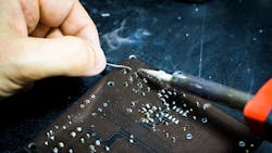
The quality of the soldering has a tremendous impact on the overall quality of the PCB. Through soldering, different parts of the PCB are connected to other electrical components to make a PCB function properly and serve its purpose. When industry professionals are evaluating the quality of electronic components and devices, one of the most prominent factors in their assessment is the caliber of the soldering work.
To be sure, soldering is quite straightforward. But it does take practice to master. As the saying goes, “practice makes perfect.” Even a complete novice can make functional solder joints. But for the overall longevity and functionality of the device, a clean and professional soldering job is the way to go.
In this guide, we’ve highlighted some of the most common problems that can happen during soldering. If you would like to know more about what it takes to make perfect solders that last, this is the guide for you.
It’s difficult to encompass all types of solder joints into one comprehensive definition. Depending on the type of solder, PCB used, or component connected to the PCB, the ideal solder joints might vary drastically. Still, most perfect solder joints have:
- Complete, solid wetting
- A smooth and shiny surface
- A neat concave fillet
To achieve an ideal solder joint, regardless of whether it’s an SMD solder joint or a through-hole solder joint, it’s necessary to use the right amount of solder, an appropriate solder iron tip heated to an accurate temperature, and a prepped PCB contact with a removed oxide layer.
Here are nine of the most common problems and mistakes that can happen on solders, usually when soldered by an inexperienced worker:
PCBs and electronic components are becoming smaller and smaller, making it difficult to maneuver around the PCB, especially when trying to solder. If you’re using a soldering-iron tip that’s too large for the PCB, you might create unwanted solder bridges.
A solder bridge is when soldering material connects two or more PCB connectors. This is quite dangerous and, if undetected, can cause the board to short circuit and burn out. Make sure to always use the right size of soldering-iron tip to prevent solder bridges.
Learn more about manufacturability issues
Novices and beginners tend to use too much solder when soldering, and a large bubble-like solder ball forms at the solder joint. Besides looking like a weird growth on the PCB, it can also be difficult to spot if the solder joint is functional. There’s plenty of room for mistakes under that ball of solder.
The best practice is to be use solder conservatively and, if necessary, add more if the joint needs it. Strive for a clean solder with a nice concave fillet.
Cold solder joints occur when the soldering iron is at a lower-than-optimal temperature, or the duration of the heating of the joint was too short. Cold solder joints have a dull, messy, pock-marked appearance. In addition, they have a shorter lifespan and are less reliable. It’s also difficult to assess whether a cold solder joint will perform well under current or limit the functionality of the PCB.
Burnt solder joints are the complete opposite of cold solder joints. It’s obvious that the soldering iron operated at a higher-than-optimal temperature, the solder joint exposed the PCB to heat way too long, or a layer of oxide was still present on the PCB, preventing optimal heat transfer. The joint has a burnt appearance, and if the pads have lifted at the joints, the PCB might be damaged beyond repair.
Tombstones often occur when trying to connect electronic components such as transistors and capacitors to the PCB. If all sides of the component are properly connected to the pads and soldered, the component will be straight.
Failing to achieve the necessary temperature for the soldering process might cause one or more sides to lift, making a tombstone-like appearance. Tombstoning affects the longevity of the solder joint and might negatively affect the thermal performance of the PCB.
One of the most frequent problems that’s causing tombstoning during the reflow soldering process is the uneven heating in the reflow oven, which can cause premature wetting of the solder in some areas of the PCB versus other areas. The uneven heating issue usually occurs for home-made reflow ovens. That’s why we recommend acquiring professional equipment.
One of the most common mistakes by beginners and novices is the lack of wetting of the solder joints. A badly wetted joint has less solder than necessary to make a proper connection between the PCB soldering pads and the electronic components attached to the PCB by solder.
Poorly wetted joints will almost certainly limit or impair the performance of the electrical device, suffer from poor reliability and longevity, and might even cause a short that could fatally damage the PCB. They also often occur when solder used in the process is insufficient.
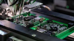
Solder skips can occur in the factory where the robots solder components to PCBs or at the hands of an inexperienced solder. It might occur due to a lack of concentration on the part of a human operator. Likewise, poorly configured robots can easily skip a joint—or one part of the joint.
This leaves the circuit open and renders certain areas or the whole PCB non-functional. Take your time and make sure to inspect all the solder joints carefully.
Lifted pads on the solder joints occur due to either excessive force or excessive heat applied to the PCB during soldering. The pad lifts off the surface of the PCB and is a potential short-circuit hazard that could ruin the whole board. Always make sure to reattach the pads back to the PCB and then solder the components on.
Webbing and splashes on the PCB occur when either the board is contaminated by pollutants that affect the soldering process or by insufficient use of the fluxing agent. Besides the messy appearance of the PCB, webbing and splashes are a huge short-circuit hazard that could potentially damage the board.
We hope that you find this guide useful and informative. If you see yourself making any of these soldering mistakes, don’t get discouraged; it happens to the best. Being an expert at soldering takes time and practice, and everyone makes mistakes.
There’s no sure-fire method to perfect soldering, but following these tips might help:
- Always inspect and familiarize yourself with the PCB before soldering.
- Make sure that the pads and joints are clean, free of pollutants, and ready for soldering.
- Keep your soldering iron in perfect shape, especially paying attention to the tip.
- Take your time.
- Practice, practice, practice.
Jonathan Bara is a PCB enthusiast, working as Marketing Manager at NeodenUSA.
About the Author
Jonathan Bara
Marketing Manager, NeodenUSA
Jonathan Bara is a PCB enthusiast, working as Marketing Manager at NeodenUSA.


