Low-Cost Substrate Supports Multiband Patch Antenna
This file type includes high resolution graphics and schematics when applicable.
Cost-effective antenna designs can be fabricated on low-cost materials, such as a durable reinforced fiberglass polymer resin material substrate. By recruiting such tools as OriginPro 8.5 software from OriginLab and the three-dimensional (3D), electromagnetic (EM) high-frequency structure simulator (HFSS) from Ansoft Corp., a compact microstrip-line-fed, H-shaped printed-circuit-board (PCB) patch antenna was designed and fabricated for multiband applications.
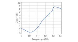
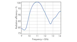
The antenna offers outstanding measured impedance bandwidth (with VSWR of less than 2.0:1) covering 3.25 GHz, from 9.75 to 13.0 GHz, with 8.5-dBi peak gain. The prototype antenna offers 0.63 dBi gain with 96% efficiency at 10.3 GHz, and 6.03 dBi gain with 84.2% efficiency at 12.5 GHz. The almost-steady radiation pattern makes the proposed antenna design suitable for X- through Ku-band applications.
The growing use of wireless technology is spurring the need for practical antenna designs.1,2 The demand for low-profile compact antennas with multiband compatibility has encouraged the development of various types of patch antennas, monopole antennas, and planar inverted-F antennas (PIFAs). Planar patch antennas, for example, are desirable for their low profiles, light weight, and simple structures.
Various dual-band antennas have been developed to save space, including circle slot antennas,3 stacked patch antennas,4 metamaterial branch line coupled antennas,5 dual-band dipole antennas,6 and slotted patch antennas on ceramic substrate material.7 Unfortunately, most of these antennas are either relatively large or lack the bandwidth for multiband use.
A considerable amount of research has been directed toward developing compact, low-cost, lightweight, planar microstrip patch antennas for multiple applications, so as to integrate with multipurpose communication modules. Antenna researchers have explored the development of compact, low-profile multiband planar antennas to meet the ever-increasing demands of smart multiple-technology wireless equipment.8
As an example, a dual-band, dual-linearly-polarized proximity-coupled patch antenna was designed with dimensions of 12.45 × 16 mm2.9 In addition, a 10 × 16 mm2 dual-band-notched square monopole antenna was proposed for ultrawideband (UWB) applications10 and a diamond dual-band antenna was designed for radio-frequency-identification (RFID) applications11; the RFID antenna features overall dimensions of 190 × 190 mm.2 Yet all of these antennas were relatively large in size, or else their performance levels were limited in gain and bandwidth.
To provide broad bandwidth in smaller antenna size, a 5-mm-long, microstrip-line-fed, inverted-H-shape, slotted patch antenna is proposed for dual-band use. Its compact size of 12 × 15 mm2 is significantly smaller than that of the other reported broadband antennas. Measurements of this proposed antenna design reveal an impedance bandwidth (with VSWR of under 2.0:1) ranging from 9.75 to 13.00 GHz (3.25 GHz), with peak gain of 8.5 dBi. The gain ranges from 0.63 dBi with 96% efficiency at the lower band at 10.3 GHz, to 6.03 dBi with 84.2% efficiency at the upper band at 12.5 GHz.
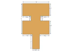
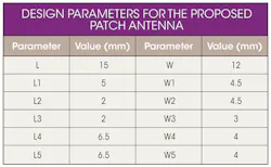
The antenna has been designed and analyzed with the aid of the three-dimensional (3D), finite-element-method (FEM) High Frequency Structure Simulator (HFSS) electromagnetic (EM) simulation software from ANSYS Corp.12Figure 1 shows the design layout for the slotted radiating patch of the proposed antenna, with the optimized parameters for the proposed antenna listed in the table.
The inverted-H-shaped radiating patch antenna was obtained by cutting slots from the conventional rectangular shape. By cutting slots, the radiating patch takes a longer path around the slots for flowing current to reach the opposite edge. The desired resonant frequency and bandwidth are achieved by introducing slots on the radiating patch.
This file type includes high resolution graphics and schematics when applicable.
Antenna Assembly
This file type includes high resolution graphics and schematics when applicable.
The proposed antenna was fabricated on low-cost, durable, 1.6-mm-thick reinforced fiberglass polymer resin substrate material. The relative permittivity of the substrate material is 4.6 with a loss tangent of 0.023. The substrate material consists of an epoxy matrix reinforced by woven glass. This composition of epoxy resin and fiberglass varies in thickness and is dependent upon direction. An attractive property of such polymer resin composites is that they can be shaped and reshaped repeatedly without losing their material properties.13
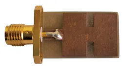
Due to the low manufacturing cost, ease of fabrication, design flexibility, and ready market availability of the proposed material, it has become a popular substrate for patch antenna design. The material is comprised of 60% fiberglass and 40% epoxy resin. Figure 2 features a photograph of the proposed antenna.
The performance of the antenna design was analyzed and optimized with the aid of FEM software and Ansoft’s HSFF EM simulator; it was plotted with the help of the OriginPro 8.5 software from OriginLab. The antenna prototype’s performance was measured in a standard far-field anechoic measurement chamber.
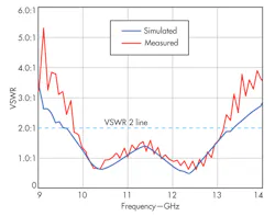
Figure 3 shows the simulated and measured VSWR of the proposed antenna. The impedance bandwidth (for a VSWR of less than 2.0:1) is 3.25 GHz, extending from 9.75 to 13.00 GHz. This shows that the lower resonance shifted from 10.5 to 10.3 GHz and the upper resonance shifted from 12.3 to 12.5 GHz. Figure 4 presents the gain achieved for the proposed antenna, from 0.6 to 6.03 dBi. Figure 5 highlights the antenna’s radiation efficiency, reaching 96% and 84.2%, respectively, at the lower and upper resonant frequencies.
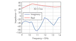
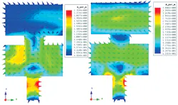
Figure 6 provides a plot of the antenna’s input impedance, with the real part of impedance optimized to be as close as possible to 50 Ω. Figure 7 shows the current distribution along the antenna’s radiating patch, revealing that the intensity of the current distribution is higher at the upper resonant frequency than at the lower resonant frequency.
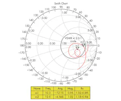
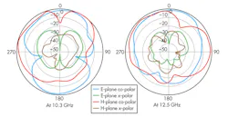
Figure 8 offers a Smith chart of the proposed antenna, validating the design’s input impedance and VSWR. The VSWR of the proposed antenna (less than 2.0:1) is within the circle. Figure 9 offers the E- and H-plane radiation patterns for the proposed antenna, with the almost steady radiation patterns at both 10.3- and 12.3-GHz resonant frequencies marking the antenna design as suitable for X- and Ku-band satellite-communications (satcom) applications.
As the results for this low-profile antenna reveal, it is capable of a 3.25-GHz impedance bandwidth with VSWR of less than 2.0:1 from 9.75 to 13 GHz using a low-cost, durable, reinforced fiber-glass polymer resin material substrate. With peak gain of 8.5 dBi, the compact slotted patch antenna measures just 15 × 12 mm, and boasts excellent performance for a variety of applications.
M. Habib Ullah, Ph.D., Research Fellow
M.T. Islam, Researcher
J.S. Mandeep, Ph.D., Professor
N. Misran, Researcher
Department of Electrical, Electronics, and System Engineering, Faculty of Engineering and Built Environment, Universiti Kebangsaan Malaysia, 43600 UKM Bangi, Selangor, Darul Ehsan, Malaysia
This file type includes high resolution graphics and schematics when applicable.
References
This file type includes high resolution graphics and schematics when applicable.
1. R. Azim, M.T. Islam, and N. Misran, “Compact Tapered-Shape Slot Antenna for UWB Applications,” IEEE Antennas and Wireless Propagation Letters, Vol. 10, 2011, pp. 1190-1193.
2. A.T. Mobashsher, M.T. Islam, and N. Misran, “A Novel High-Gain Dual-Band Antenna for RFID Reader Applications,” IEEE Antennas and Wireless Propagation Letters, Vol. 9, 2010, pp. 653-656.
3. R. Emadian, M. Mirmozafari, C. Ghobadi, and J. Nourinia, “Bandwidth enhancement of dual band-notched circle-like slot antenna,” Electronics Letters, Vol. 48, No. 7, 2012, pp. 356-357.
4. M.H. Ullah, M.T. Islam, M.S. Jit, and N. Misran, “A three-stacked patch antenna using high-dielectric ceramic material substrate,” Journal of Intelligent Material Systems and Structures, Vol. 23, No. 16, 2012, pp. 1827-1832.
5. Y.-K. Jung and B. Lee, “Dual-Band Circularly Polarized Microstrip RFID Reader Antenna Using Metamaterial Branch-Line Coupler,” IEEE Transactions on Antennas and Propagation, Vol. 60, No. 2, 2012, pp. 786-791.
6. W.X. An, H. Wong, K.L. Lau, S.F. Li, and Q. Xue, “Design of Broadband Dual-Band Dipole for Base Station Antenna,” IEEE Transactions on Antennas and Propagation, Vol. 60, No. 3, 2012, pp. 1592-1595.
7. M.H. Ullah, M.T. Islam, and J.S. Mandeep, “Ceramic Substrate Shrinks Patch Antenna,” Microwaves & RF, Vol. 51, No. 8, 2012, pp. 50-54.
8. J.J. Tiang, M.T. Islam, N. Misran, and J.S. Mandeep, “Circular microstrip slot antenna for dual-frequency RFID application,” Progress In Electromagnetics Research, Vol. 120, 2011, pp. 499-512.
9. M. Veysi, M. Kamyab, and A. Jafargholi, “Single-Feed Dual-Band Dual-Linearly-Polarized Proximity-Coupled Patch Antenna,” IEEE Antennas and Propagation Magazine, Vol. 53, No. 1, 2011, pp. 90-96.
Related Articles
• RF Materials Can Open The Gates For Next-Generation Technology
• Interview: Bob Giometti, SkyCross
• Planar Antenna Aids UWB Communications
10. M. Mehranpour, J. Nourinia, C. Ghobadi, and M. Ojaroudi, “Dual Band-Notched Square Monopole Antenna for Ultrawideband Applications,” IEEE Antennas and Wireless Propagation Letters, Vol. 11, 2012, pp. 172-175.
11. M.I. Sabran, S.K.A. Rahim, A.Y.A. Rahman, T.A. Rahman, M.Z.M. Nor, and Evizal, “A Dual-Band Diamond-Shaped Antenna for RFID Application,” IEEE Antennas and Wireless Propagation Letters, Vol. 10, 2011, pp. 979 –982.
12. M.H. Ullah, M.T. Islam, and J.S. Mandeep, “Printed prototype of a wideband S-shape microstrip patch antenna for Ku/K band applications,” Journal of the Applied Computational Electromagnetics Society, Vol. 28, No. 4, 2013, pp. 307-317.
13. M.H. Ullah, M.T. Islam, J.S. Mandeep, and N. Misran, “A New Double L Shape Multiband Patch Antenna on Polymer Resin Material Substrate,” Applied Physics A: Materials Science & Processing 2012, DOI: 10.1007/s00339-012-7114-0.
This file type includes high resolution graphics and schematics when applicable.


