Low-Power Mixer Converts UWB Signals
This file type includes high resolution graphics and schematics.
Ultrawideband (UWB) communications has been in use for military and various niche applications for more than 20 years.1 But in February 2002, the United States’ Federal Communications Commission (FCC) allocated a generous 7500 MHz of bandwidth from 3.1 to 10.6 GHz for unlicensed use of UWB devices, opening up a potentially large market. UWB technology can provide many benefits for commercial applications, including operation at low power and low cost at high data rates and with reduced interference. The low-voltage and low-power operation of UWB devices enable mobile wireless communications transceivers to be reduced in size and weight,2 although the use of low supply voltages presents challenges for some of the analog circuit portions of UWB designs.3 The frequency mixer, for example, is a critical part of UWB applications.4 It must translate incoming RF signals to an intermediate-frequency (IF) range that can be handled by data converters.5
Related Articles
• UWB Antenna Blocks Interference
• UHF/UWB Antenna Supports Indoor Tracking
• Accurately Model UWB Antenna Pulses
Double-balanced Gilbert-cell mixers are among the more popular of active mixer types, owing to their low noise, high gain, high port-to-port isolation, and simplicity. These technology-independent mixers can be realized in a number of different semiconductor processes—among them, the use of silicon CMOS or bipolar processes. Still, designing low-voltage, low-power Gilbert-cell mixers at RF/microwave frequencies is challenging due to the stacking of transistors between supply and ground. Also, the mixer’s transistors typically operate in the saturation region which increases current dissipation. A new approach is clearly needed to create a low-power mixer suitable for UWB requirements.
Some low-voltage, low-power mixer topologies using CMOS technology have been proposed in recent years.6-11 A low-voltage topology using inductor-capacitor (LC) tanks was reported in ref. 6. This approach allows for low-power operation, but the inductor occupies a large area on the chip (1.5 x 1.1 mm2) and yields narrowband operation (2.4 GHz). In ref. 7, a modified Gilbert-type mixer achieved low power consumption using triode operation and shunt capacitors at the local-oscillator (LO) switching stage but, again, this was a narrowband circuit. In ref. 8, DC power consumption was held to 500 μW by operating the mixer’s CMOS transistors in the subthreshold region. But because the bias current is so low, the noise performance was poor, with a double-sideband (DSB) noise figure (NF) of 18.3 dB.
On-chip transformers can also be used to lower the supply voltage in mixers, and such an approach was adopted in ref. 9 with low DC power consumption. However, the mixer’s 3-dB bandwidth was relatively narrow (2.1 to 3.0 GHz) because of the bandwidth limitation of the transformer.
Mixers using a Gilbert folded topology or with a switched-transconductance topology10,11 are good choices for low-voltage applications. That said, the current consumption is generally twice that of a conventional Gilbert cell mixer, making the power consumption similar to that of a conventional Gilbert cell mixer. Current bleeding can improve the mixer noise figure, since less current will flow at the LO switching stage.12 Since parasitic capacitances are increased by a bleeding circuit, however, it indirectly generates more noise. To eliminate the effects of the parasitic capacitance, resonating inductors could be used, although this would increase chip size while decreasing bandwidth.13
This file type includes high resolution graphics and schematics.
A Different Approach
This file type includes high resolution graphics and schematics.
To overcome these limitations of traditional low-voltage, low-power mixer approaches, a mixer was designed with bulk-injection, DTMOS, and switched-biasing techniques for applications from 0.6 to 11.0 GHz. The bulk-injection technique combines the RF transconductance stage with the LO switching stage to reduce the number of stacked transistors, providing flat conversion gain over a wide frequency range with low DC power consumption. Unfortunately, the bulk-injection approach exhibits relatively high NF. To reduce flicker noise and white noise, a switched-biasing technique with DC level shifting circuits was adopted in the new mixer design.
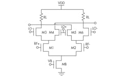
Figure 1 shows a conventional Gilbert-cell double-balanced mixer. It contains four stages: tail current source (transistor M8), RF transconductance stage (transistors M1, M2), LO switching stage (transistors M3-M6), and output load stage (resistor RL). Devices M1 and M2 transconduct differential RF input signals into small-signal drain currents. These currents are then switched by transistors M3-M6 as a function of the local oscillator (LO) signal, thus performing performs frequency conversion.
1. This schematic diagram represents a conventional Gilbert cell double-balanced mixer.
For the circuit of Fig. 1 to operate as intended, the supply voltage (VDD) must be high enough to maintain the tail current source transistor (MB), the RF transconductance transistors (M1, M2), and the LO switching transistors (M3-M6) in saturation, while taking into account the voltage drop across the load resistor (RL). Because of the high minimum supply-voltage requirement in a Gilbert-cell mixer, low-voltage operation is difficult to achieve.
The proposed new mixer is based on the body effect that occurs when a device gate terminal is used as an input signal terminal. To understand this effect, when the gate terminal of a transistor (in a mixer circuit) is fed by an LO signal, the drain-source current, IDS, can be expressed by Eq. 1:
IDS = K(W/L)( VGS - VTH) (1)
where:
K = a proportionality constant;
W = the transistor gate width;
L = the transistor gate length;
VGS = the voltage between the transistor’s gate and source; and
VTH = the threshold voltage of the transistor.
Since VTH is a function of the voltage between the bulk material and the source, VBS, to a first-order approximation, VTH, can be written in the form of Eq. 2:
VTH(LO) = VTO + γ[2φF - VBS(LO)]0.5 - γ(2φF)0.5 (2)
where:
VT0 = the zero substrate bias threshold voltage, where the typical value of VT0 is about 0.5 V in a 0.18-μm silicon CMOS semiconductor process;
φF = the surface potential; and
γ = the body effect factor.
From Eqs. 1 and 2, the only parameter available to the designer for threshold voltage manipulation is the bulk-source voltage, VBS. The LO signal as a function of bulk-to-source voltage is injected into the bulk of the transistors, and the threshold voltage is then modulated with the LO signals.14 If the gate of the transistor is biased close to the threshold voltage and the LO signal swing is large enough, the transistors of the bulk-injection core stage will turn on and off as a function of the LO signal.
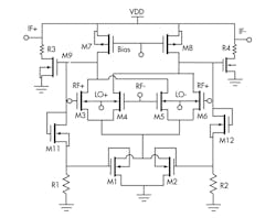
Figure 2 shows the complete circuit diagram of the proposed mixer, with the output buffer and mixer core. The mixer consists of five parts: the switched-biasing stage (containing transistors M1, M2); the bulk-injection core stage (M3-M6); the load stage (M7, M8); the output buffers (M9, M10 and R3, R4); and the DC level shifting circuits (M11, M12 and R1, R2).
2. This schematic diagram represents the proposed mixer.
This file type includes high resolution graphics and schematics.
Bulk-Source Particulars
This file type includes high resolution graphics and schematics.
Other mixer designs have employed the bulk-injection concept. The circuit in ref. 15 applies the RF signal to the transistor bulk portion and the LO signal to the gate; this produces lower gain, since the bulk-source transconductance is much lower than the gate-source transconductance. The design in ref. 16 uses PMOSFETs (for isolation), as the process used for that design did not support the deep n-well option.
In contrast to a conventional Gilbert-cell mixer, the bulk-injection core stage merges the RF transconductance stage with the LO switching stage. Since it has one less stacked stage than a Gilbert-type mixer, the proposed mixer can operate with a lower supply voltage. In addition, the gate-source voltage of the core transistors (M3-M6) is lower than the threshold voltage (VGS = 0.45 V) in order to operate in the subthreshold region, resulting in low current dissipation.
The PMOS transistors (M7, M8) and their high output impedances are used as an active load to transfer current to voltage for the mixer’s intermediate frequency (IF) output signals. Moreover, the PMOS active load can reduce the alternating current (AC) flow through the mixer core and lower the voltage drop on the active load. The supply voltage (VDD) can also be lower; in this mixer, the optimum value of VDD is 0.7 V.
The buffer stage consists of two common-source NMOS amplifiers, defined by M9, M10, R3, and R4 in Fig. 2. The buffer stage achieves the impedance matching for driving a 50-Ω load and offers sufficient power gain to maintain positive gain in the new mixer design.
A mixer following a low noise amplifier (LNA) is an important building block in a wireless communications system, and a mixer with high noise will increase the noise figure of the overall system.17 In addition to white thermal noise, MOS transistors are notorious for flicker (or 1/f) noise. In general, the 1/f noise performance of a mixer is primarily determined by the LO switching pairs. Conventional flicker-noise-reduction techniques generally lead to higher power consumption.
For the proposed mixer, a switched-biasing technique is employed to improve the mixer’s noise performance and reduce the power consumption. This approach has been applied to lower the flicker noise is a switched biasing technique at the tail current circuit; it was initially adopted to improve phase noise in voltage-controlled-oscillator (VCO) circuits.18
The switched-biasing technique tackles the 1/f noise problem by cycling a MOS transistor between strong inversion and accumulation regions. The technique reduces both flicker and white noise. When the flicker noise from an MOS transistor that is due to the current source can be reduced, the NF of the mixer can be improved. Additionally, by using self-biasing with the drain output signal of transistors M7 and M8 to drive the tail current transistors, the mixer does not require supplementary bias circuits. It is capable of reducing power consumption, as well as current source variations from supply-voltage and temperature effects in bias circuits.
In general, a low NF is most critical for low input power levels. However, any NF improvement from the switched-biasing technique will be minimal under low signal power. As Fig. 2 shows, DC level shifting circuits are composed of M9, M10, R1, and R2 to provide the tail current transistors; a proper gate-source voltage makes the overdrive voltage (VOV = VGS - VTH) very small for the symmetric switching operation with a small output swing.
Figure 2 also shows that transistors M1 and M2 are dynamic-threshold-voltage MOS (DTMOS) devices, a configuration obtained by tying the gate and the bulk of a MOSFET together. In this approach, the threshold voltage of the MOS transistor is a function of its gate voltage—i.e., as the gate voltage increases, the threshold voltage drops, resulting in much higher drive current than in a standard MOSFET.19
The DTMOS approach supports low-voltage applications. A DTMOS device can have a high threshold voltage at gate-to-source voltage equal to zero. Therefore, the leakage current is low. At gate-to-source voltage equal to VDD, the threshold voltage is low and the device can achieve high speed. This dynamic variability is beneficial for low power consumption at very low voltage.
This file type includes high resolution graphics and schematics.
Finding The Middle Ground
This file type includes high resolution graphics and schematics.
In most RF front ends, a mixer follows an LNA, and should provide high linearity, low noise, and adequate gain to overcome the noise levels of the IF and baseband sections that follow. From a designer’s perspective, the main challenge in active mixer design is optimizing conversion gain, linearity, and NF simultaneously. According to Fig. 2, the mixer’s small-signal gain can be expressed by Eq. 3:
Gain = -gm(RO-NMOS x RO-PMOS) (3)
and the mixer’s conversion gain (CG) can be expressed by Eq. 4:
CG = (-2/π)gm(RO-NMOS x RO-PMOS) (4)
where:
VIF = the IF output voltage;
VRF = the RF input voltage;
2/π = the factor for a square-wave LO signal;
gm = the transconductance of the NMOS transistor;
RO-NOMS = the output resistance of the NMOS transistor; and
RO-PMOS = the output resistance of the PMOS transistor.
Transconductance, gm, can be expressed by Eq. 5:
gm = ∂iD/∂VGS = (KRFID)0.5 (5)
where the process parameter, KRF, can be found from Eq. 6:
KRF = 2μnCOX(W/L) (6)
where:
ID = the drain current;
KRF = a process parameter;
μn = the carrier mobility;
COX = the gate-oxide capacitance per unit area;
W = the width of the core transistors (M3 - M6); and
L = the length of the core transistors (M3 - M6).
Drain current ID is set by the tail current transistors (M1, M2). From Eq. 4, it can be seen that the CG is proportional to the transconductance, gm, of the core transistors (M3 - M6). To achieve sufficient transconductance and high CG, a large gate width is required for these transistors. The optimal size of the core transistors is with a gate width of 89 μm and gate length of 0.18 μm.
For a transceiver, particularly in wireless communications systems, linearity is a key performance parameter. The linearity of a system’s mixer will have a significant impact on the overall linearity of the system. The linearity in terms of input-third-order intercept point (IIP3) can be expressed as Eq. 7:
IIP3 = 4[(2/3)(ID/KRF)]0.5 (7)
Equation 7 indicates that an increase in drain current should improve the mixer’s linearity. However, the voltage drop across the active load (M7, M8) is also increased. This in turn reduces the available voltage headroom at the output of the mixer for a fixed supply voltage, thereby deteriorating the overall mixer performance. To achieve acceptable linearity performance with high gain and low noise figure, the proposed mixer consumes approximately 1.02 mA (255 μA) for each of the four core transistors).
Because the bulk-injection technique degrades mixer NF, switched biasing is also used with this mixer to improve its noise performance. Two major mechanisms generate 1/f noise of the switching pairs. One is a direct mechanism, owing to the finite slope of the switching pair transitions. The LO switching generates noise pulse trains by the direct mechanism. The DC average of noise pulse trains is the output flicker-noise current, as described by Eqs. 8 and 913:
io,n(dir) = (4I x Vn/(S x T) (8)
Vn = [2x( Kf/ WeffLeffCoxf)]0.5 (9)
where:
I = the bias current for the RF transconductance stage;
T = the LO period;
Vn = the equivalent flicker noise of the switching pair;
S = the slope of the LO signal;
Weff = the effective width of the device;
Leff = the effective length of the device;
Cox = the oxide capacitance;
f = the frequency; and
Kf = a process parameter.13
The other mechanism that generates 1/f noise is an indirect mechanism, as flicker noise mainly depends on the tail capacitance of the node between the LO switches and RF transconductance stage.11 When a sinewave LO is applied to the mixer, the average of the output noise current generated by the indirect mechanism is expressed by Eq. 1013:
io,n(ind) = (2CP/T)Vnx (CPwLO)2/[g2ms + (CPwLO)2)] (10)
where:
CP = the tail capacitance of the node between the LO switches and the RF transconductance stage;
T = the LO period;
gms = the transconductance of the LO switches; and
Vn = the equivalent flicker noise of the switching pair.
The NF of the proposed mixer can be expressed as Eq. 11:
where:
Vn, IN = the input noise voltage;
Vn, OUT = the total output noise voltage; and
Vn, CIR = the circuit-added output noise voltage.
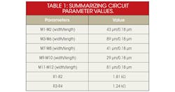
From Eq. 10, it can be seen that the mixer’s NF is inversely proportional to its conversion gain. Table 1 summarizes some of the key circuit parameters for the design.
This file type includes high resolution graphics and schematics.
Put To The Test
This file type includes high resolution graphics and schematics.
The UWB mixer was simulated and designed with the aid of the Advanced Design System (ADS) simulation software from Agilent Technologies. It was fabricated with the 0.18-μm RF silicon CMOS semiconductor process fromTaiwan Semiconductor Manufacturing Company (TSMC). By employing bulk-injection and DTMOS techniques, the mixer’s supply voltage falls to 0.7 V and consumes only 0.71 mW power.
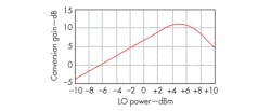
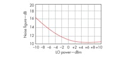
Simulated CG versus LO input power is plotted in Fig. 3, which shows maximum CG of 11.3 dB with an LO input power of +5 dBm and RF power of -30 dBm. Figure 4 shows the double-sideband (DSB) NF as a function of LO input power. From Fig. 4, it can be seen that the minimum NF can be achieved when LO input power is equal to +5 dBm, revealing that maximum conversion gain and minimum NF occur for LO input power level of +5 dBm.
3. The proposed mixer’s conversion gain is shown as a function of LO input power.
4. The new mixer’s double-sideband (DSB) noise figure is shown versus LO input power.
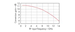
Figure 5 shows CG for RF input signals swept from 0.6 to 14 GHz. As Fig. 5 indicates, the mixer’s 3-dB RF bandwidth extends from 0.6 to 11.0 GHz (a 10.4-GHz 3-dB bandwidth) with a fixed IF output of 100 MHz. The optimum DC supply voltage (VDD) is about +0.7 VDC with a 1.02 mA drain current, and the output buffers consume less than 0.02 mW for all measured results.
5. The proposed mixer’s conversion gain is plotted here as a function of RF input frequency.
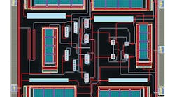
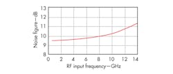
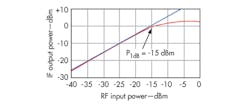
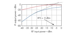
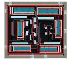
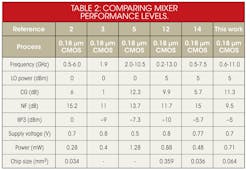
Figure 6 shows the DSB NF versus RF input frequency, which is 9.51 to 10.45 dB from 0.6 to 11.0 GHz. Figure 7 shows that the input 1-dB compression point (P1dB) is approximately -15 dBm. Figure 8 shows the IIP3 performance, with simulated IIP3 of -5 dBm. Figure 9 shows the mixer’s circuit layout, with total chip area of 0.29 x 0.22 mm2, including the input and output pads. Table 2 summarizes the mixer’s performance, with comparisons to earlier designs.
6. The mixer’s double-sideband (DSB) noise figure is plotted here as a function of RF input frequency.
7. This plot shows the 1-dB-compression-point performance of the proposed mixer.
8. This plot shows the input-third-order-intercept (IIP3) performance of the proposed mixer.
9. This photograph shows the circuit layout for the new mixer.
This file type includes high resolution graphics and schematics.
The Bottom Line
This file type includes high resolution graphics and schematics.
In summary, the proposed downconversion mixer achieves a 3-dB bandwidth of 0.6 to 11.0 GHz, with maximum CG of 11.3 dB and minimum NF of 9.5 dB. Fabricated with a commercial 0.18-μm silicon CMOS process, the low-power mixer hits a 1-dB compression point of -15 dBm with IIP3 of -5 dBm, while consuming only 0.71 mW from a +0.7-VDC supply. It is well suited for frequency conversion in battery-powered, UWB communications devices.
Related Articles
• UWB Antenna Blocks Interference
• UHF/UWB Antenna Supports Indoor Tracking
• Accurately Model UWB Antenna Pulses
Acknowledgements
This work was supported in part by the Open Fund Project of Key Laboratory in Hunan Universities (No. 12K012). The authors would also like to thank the anonymous reviewers for their invaluable suggestions, which helped improve the quality of the article.
Jian Liu, M.S. Degree Candidate
Chunhua Wang, Professor, Doctoral Supervisor
College of Information Science and Engineering, Hunan University, Changsha 410082, Hunan Province, People’s Republic of China; e-mail: [email protected].
References
1. G. Roberto Aiello and Gerald D. Rogerson, “Ultra-wideband Wireless Systems,” IEEE Microwave Magazine, June 2003, pp. 36-47.
2. K.-H. Liang and H.-Y. Chang, “0.5-6 GHz low-voltage low-power mixer using a modified cascade topology in 0.18-μm CMOS technology,” IET Microwaves, Antennas & Propagation, Vol. 5, No. 2, 2011, pp. 167-174.
3. M.J. Deen, R. Murji, A. Fakhr, N. Jafferali, and W.L. Ngan, “Low-power CMOS integrated circuits for radio frequency applications,” IEE Proceedings on Circuits, Devices, and Systems, Vol. 152, No. 5, October 2005, pp. 509-522.
4. M.M. Reja, K. Moez, and I. Filanovsky, “A Novel 0.6-V CMOS Folded Gilbert-Cell Mixer for UWB Applications,” IEEE International SOC Conference, September 17-20, 2008, pp. 169-172.
5. M. Tavassoli, E. Kargaran, S. Izadpanah Tous, and H. Nabovati, “Design of 0.5-V, 1.28-mW CMOS UWB mixer using the body effect,” in IEEE 55thInternational Midwest Symposium on Circuits and Systems (MWSCAS), August 5-8, 2012, pp. 202-205.
6. Chih-Chun Tang, Wen-Shih Lu, Lan-Da Van, and Wu-Shiung Feng, “A 2.4-GHz CMOS Down-Conversion Doubly Balanced Mixer with Low Supply Voltage,” in IEEE International Symposium on Circuits and Systems (ISCAS), Vol. 4, May 6-9, 2001, pp. 794-797.
7. J.-D. Chen, Z.-M. Lin, and J.-S. Row, “A 2-GHz low-power down-conversion mixer in 0.18 μm CMOS technology,” IEICE Transactions on Electronics, Vol. E91-C, No. 1, January 2008, pp. 64-71.
8. H. Lee and S. Mohammadi, “A 500-μW, 2.4-GHz CMOS Subthreshold Mixer for Ultra Low Power Applications,” IEEE RFIC Symposium, June 3-5, 2007, pp. 328-328.
9. C. Hermann, M. Tiebout, and H. Klar, “A 0.6-V, 1.6-mW Transformer-Based 2.5-GHz Downconversion Mixer With +5.4-dB Gain and -2.8-dBm IIP3 in 0.13-μm CMOS,” IEEE Transactions on Microwave Theory & Techniques, Vol. 53, No. 2, February 2005, pp. 488-495.
10. V. Vidojkovic, A. van der Tang, A. Leeuwenburgh, and A.H.M. van Roermund, “A Low-Voltage Folded-Switching Mixer in 0.18 μm CMOS,” IEEE Journal of Solid-State Circuits, Vol. 40, No. 6, June 2005, pp. 1259-1264.
11. Eric A.M. Klumperink, Simon M. Louwsma, Gerard J.M. Wienk, and Bram Nauta, “A CMOS Switched Transconductor Mixer,” IEEE Journal of Solid-State Circuits, Vol. 39, No. 8, August 2004, pp. 1231-1240.
12. Myoung-Gyun Kim, Hee-Woo An, Yun-Mo Kang, Ji-Young Lee, and Tae-Yeoul Yun, “A Low-Voltage, Low-Power, and Low-Noise UWB Mixer Using Bulk-Injection and Switched Biasing Techniques,” IEEE Transactions on Microwave Theory & Techniques, Vol. 60, No. 8, August 2012, pp. 2486-2493.
13. Jinsung Park, Chang-Ho Lee, Byung-Sung Kim, and J. Laskar, “Design and Analysis of Low Flicker-Noise CMOS Mixers for Direct-Conversion Receivers,” IEEE Transactions on Microwave Theory & Techniques, Vol. 54, No. 12, December 2006, pp. 4372-4380.
14. Kung-Hao Liang, Hong-Yeh Chang, and Yi-Jen Chan, “A 0.5-7.5 GHz Ultra Low-Voltage Low-Power Mixer Using Bulk-Injection Method by 0.18-μm CMOS Technology,” IEEE Microwave & Wireless Component Letters, Vol. 17, No. 7, July 2007, pp. 531-533.
15. G. Kathiresan and C. Toumazou, “A Low Voltage Bulk Driven Downconversion Mixer Core,” IEEE International Symposium on Circuits & Systems, Vol. 2, July 1999, pp. 598-601.
16. Hong Mo Wang, “A 1-V Multigigahertz RF Mixer Core in 0.5-μm CMOS,” IEEE Journal of Solid-State Circuits, Vol. 33, No. 12, December 1998, pp. 2265-2267.
17. M. Kim, J. Lee, and T. Yun, “Low-noise and high-gain mixer combining switched-biasing and current-bleeding techniques,” Electronics Letters, Vol. 48, No. 23, November 2012, pp. 1476-1478.
18. Eric A.M. Klumperink, Sander L.J. Gierkink, Arnoud P. van der Wel, and Bram Nauta, “Reducing MOSFET 1/f Noise and Power Consumption by Switched Biasing,” IEEE Journal of Solid-State Circuits, Vol. 35, No. 7, July 2000, pp. 994-1001.
19. F. Assaderaghi, D. Sinitsky, S.A. Parke, J. Bokor, P.K. Ko, and Hu Chenming, “Dynamic Threshold-Voltage MOSFET (DTMOS) for Ultra-Low Voltage VLSI,” IEEE Transactions on Electron Devices, Vol. 44, No. 3, March 1997, pp. 414-422.
This file type includes high resolution graphics and schematics.
