Novel LC Tank Steers Low-Power VCO
This file type includes high resolution graphics and schematics when applicable.
Implementing low-power voltage-controlled-oscillator (VCO) circuitry with high-frequency silicon CMOs semiconductor technology can provide effective signal generation for a wide range of wireless applications. By adopting a VCO design with an inductive-capacitive (LC) tank circuit, the oscillator can achieve outstanding performance at RF/microwave frequencies while minimizing the supply voltage.
Related Articles
• VCO Cuts Noise At 3850 MHz
• VCO Tunes From 902 To 928 MHz
• VCO Tunes At 6 GHz
Typically, tradeoffs are required when designing a VCO for low power consumption, a wide frequency tuning range, and low phase noise, and a number of low-power CMOS oscillators have been reported for applications operating at less than 1 V.1-5 These designs typically sacrifice in output power or phase noise at their low operating voltages. Fortunately, a VCO with tuning range of better than 40% has been achieved in silicon CMOS, tuning 2.21 to 3.33 GHz with 0 to +0.8 VDC and consuming only 0.248 mW power for a supply voltage of less than +0.8 VDC while maintaining low phase noise.
Many of the earlier CMOS oscillators suffer from reduced output swing and degraded phase noise because of the limited supply voltage. Improvements in output swing and phase noise have been achieved by incorporating capacitive feedback and forward-body-bias (FBB) techniques in a cross-coupled CMOS VCO approach.6 Unfortunately, the frequency tuning range is still relatively narrow due to the limited supply voltage. Two techniques have typically been used to increase the tuning range: capacitive and inductive coarse tuning techniques. The capacitive coarse tuning approach is based on the variation of the capacitive part of the LC tank circuit,7-11 while the inductive coarse tuning methods is based on varying the inductive part of the LC tank circuit.12-16
Compared to the switched capacitor approach, the main drawbacks of the inductive coarse tuning techniques are related to a higher degradation of the overall LC tank quality. Moreover, the additional parasitic capacitance introduced by a variable inductor must be minimized to preserve the tuning range. The advantages of switched-capacitor coarse tuning techniques include a small VCO gain parameter, KVCO, and a wide frequency tuning range. A wide variation between the minimum gain parameter, KVCO min, and maximum gain parameter, KVCO max, can impact VCO performance in several ways.17
A wide variation in the gain parameter can affect phase noise in the lower or middle parts of the oscillator frequency range, assuming the varactor stage does not constantly amplify the different noise sources (1/f and thermal noise from sustaining amplifier transistors and bias stage). In phase-locked-loop (PLL) applications, large variations in KVCO could lead to PLL instability due to variations in its open-loop gain, as well as degradation in closed-loop integrated phase noise and settling time.
The current solution involves achieving a wide frequency tuning range with a small value of KVCO. This wideband, low-power VCO exploits an integrated LC tank based on the use of a FBB technique and switched capacitor array. The novel topology and use of FBB result in changes in threshold voltage with changes in body-bias voltage, making it possible to achieve a lower threshold voltage for given operating conditions. By using a switched capacitor bank, it is possible to achieve a wide frequency tuning range.
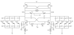
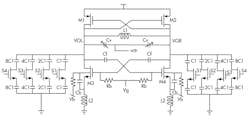
Figure 1 shows a schematic diagram of the proposed VCO, with its cross-coupled complementary topology. This approach yields robust start-up operation and lower 1/f noise compared to NMOS-only VCOs. To reduce the supply voltage required, the tail current transistor in a conventional cross-coupled VCO has been replaced in this design by on-chip inductors.18 As a result, the DC voltage drop over the inductors becomes negligible, allowing the source node to swing below ground and leave maximum voltage headroom for the oscillating signal.
The inductors are tuned to provide the source nodes of devices M3 and M4 with high impedances at twice the oscillation frequency, to reduce phase noise. These inductors contribute very little noise. The supply voltage for the cross-coupled complementary device pair is +0.8 VDC; the resonator consists of a spiral inductor, a pair of AC-coupled accumulation mode varactor diodes, and a switched capacitor array.
This file type includes high resolution graphics and schematics when applicable.
Assembly
This file type includes high resolution graphics and schematics when applicable.
Figure 2 shows the input resistance of a cross-coupled transconductor (devices M3 and M4) and its equivalent circuit. The following equations are based on the equivalent circuit:
vin = vgs4 - vgs3 (1)
iin = gm3 vgs3 = gm4 vgs4 (2)
According to Eqs. 1 and 2, the equivalent negative resistance, rin,n, can be derived by Eq. 3:
rin,n = vin/ iin = 1/gm3 - 1/gm4 (3)
where:
gm3 = the transconductance of M3 and
gm4 = the transconductance of M4.
Assuming that gm3 = gm4 = gmn, then
rin,n = vin/ iin = -2/gmn (4)
In the same way, it is easy to get rin,p, the negative resistance of devices M1 and M2:
rin,p = vin/iin= -2/gmp (5)
The total LC tank parallel negative resistance is
rtotal = -2/( gmn + gmp) (6)
For startup, the total negative resistance exhibited by the transconductances M1-M2 and M3-M4 must be less than the parallel parasitic resistance of the LC resonator—namely, Eq. 7:
rtotal = 2/(gmn + gmp) < rp (7)
where:
rp = the LC parallel resonant circuit equivalent resistance.
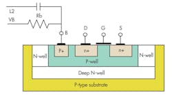
As Fig. 3 depicts, for deep-submicrometer MOSFETs, the threshold voltage is no longer constant. Nevertheless, it can be manipulated by the DC bias at the body terminal, adding one more degree of freedom to circuit designs. Typically, the threshold voltage of an n-channel MOSFET is given as19:
Vt = Vt0 + γ[(2ΦF + VSB)0.5 -(2ΦF)0.5] (8)
where:
Vt0 = the threshold voltage for VSB = 0;
VSB = the source-to-body voltage;
ΦF = a semiconductor parameter with typical value in the range of 0.3 to 0.4 V; and
γ = a process-dependent parameter.
To suppress the negative influence from body transconductance, capacitor Cb is inserted between the source terminals and body terminal. The current-limiting resistor, Rb, is included at the body terminal to prevent excessive junction conduction.
According to Eq. 8, if the value of VSB has changed, the threshold voltage will also change, as the source terminal of the NMOS device is connected to inductor L2 and voltage VS is almost close to 0 V. The value of threshold voltage Vt can be changed by adding different body-bias voltage, Vb. At the same time, as the drain current associated with the value of VGS - Vt, namely ID, is controlled by the voltage difference of VGS - Vt, while Vt changes with the change of Vb, the value of Vg is adjusted according to the change in threshold voltage to maintain current ID at a constant value.
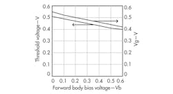
In this way, this novel topology can operate with very low power consumption. Figure 4 shows simulated effective threshold voltage and Vb. These simulated results show that once the FBB voltage Vb increases by 100 mV, the threshold voltage will decrease by almost 19 mV.
Tunable oscillator operation is vital to many modern applications. In the current VCO design, the VCO gain parameter, KVCO, determines the VCO’s phase-noise performance and loop characteristics of a PLL circuit. For low phase noise, it is usually desirable to have a value of KVCO as low as possible, although a small value of KVCO also means a narrow frequency tuning range. To extend the frequency tuning range for a design with small value of KVCO, a switched capacitor array is used in the current design (Fig. 5).
The switched capacitor array is implemented with nMOS devices since the 1/f noise models for nMOS devices were found to be more accurate than those for pMOS models. The aspect ratio of the switching transistors should be as large as possible so that they operate mostly in the triode region where the noise characteristics are lower, but not so large that their parasitic capacitances limit the tuning capability of the VCO.
This file type includes high resolution graphics and schematics when applicable.
Summing Up
This file type includes high resolution graphics and schematics when applicable.
Based on the switched capacitor array, the oscillation frequency of the LC-tank VCO is defined by Eq. 9:
fosc = 1/2π[L(Cv + Carray + Cpar]0.5 (9)
where:
Cpar = the parasitic capacitance,
Carray = the switchable capacitor bank, and
Cv = the capacitance value of the varactor.
The oscillator frequency, fosc, is coarsely controlled by Carray and finely tuned by Cv, with its value determined by the control voltage, Vctr. The VCO gain, KVCO, can be derived using Eq. 10:
KVCO = ∂fosc/∂Vctr = -[1/4π√L(Cv + Carray + Cpar1.5] × (∂Cv/∂Cvctr) (10)
It can be shown from Eq. 10 that KVCO is a strong function of the capacitance of the switched capacitor array. The use of the switched capacitor array not only broadens the VCO frequency tuning range but also results in a more ideal value for KVCO.
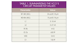
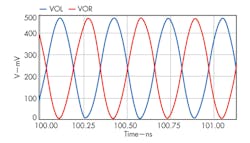
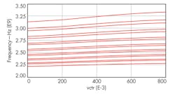
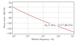
The proposed LC VCO design of Fig. 1 was fabricated with an 0.18-μm silicon CMOS semiconductor technology. Table 1 lists the parameters for the VCO’s components. Figure 6 shows the differential output voltage swing of the VCO core. The circuit draws DC current of 0.310 mA from a +0.8-VDC supply, which means the proposed VCO topology has DC power consumption of 248 μW. Figure 7 shows the measured frequency tuning curves. The 16 overlapping tuning curves cover the desired frequencies with sufficient overlaps between adjacent bands and with good tuning linearity. The VCO circuit exhibits a tuning range of 40.1% from 2.21 to 3.33 GHz with tuning voltages ranging from 0 to +0.8 VDC. Figure 8 shows that the VCO achieves phase noise of -112.7 dBc/Hz at a far offset of 1 MHz from a 3.33-GHz carrier.
A figure-of-merit (FOM) parameter was used to evaluate the three performance parameters for VCO: frequency, phase noise and power consumption, defined by Eq. 11:
FOM = Lfoffset - 20log(f0/foffset) + 10log[PDC/(1 mW)] (11)
where P, the power dissipated by the oscillator core (in mW), L(Δω, is the total single-sideband (SSB) phase-noise spectral density at offset frequency Δω from the carrier, Ω0, with a higher value of the FOM implying better performance.
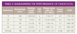
Based on these parameters and calculations, the performance of this novel VCO design is presented in Table 2, alongside of recent oscillator developments and their performance levels. As Table 2 shows, the new VCO features the lowest power consumption of all the oscillators. As can be seen in the other designs, power consumption is traded off for phase noise performance, frequency turning range, and the output swing.
Acknowledgments
This work was supported in part by the Open Fund Project of Key Laboratory at Hunan University (No. 12K012). The authors would like to thank the anonymous reviewers for their valuable suggestions, which helped improve the quality of the article.
Jianqun Ding, Master’s Degree Candidate
Chunhua Wang, Professor and Doctoral Supervisor
Xiaorong Guo, Associate Professor
Wen Weng, Master’s Degree Candidate
College of Information Science and Engineering, Hunan University, Changsha 410082, People’s Republic of China
This file type includes high resolution graphics and schematics when applicable.
References
This file type includes high resolution graphics and schematics when applicable.
1. H.-H. Hsieh, K.-S. Chung, and L.-H. Lu, “Ultra-low-voltage mixer and VCO in 0.18-μm CMOS,” in IEEE Radio Frequency Integrated Circuits Symposium, June 2005, pp. 167–170.
2. K. Kwok and H. C. Luong, “Ultra-low-voltage high-performance CMOS VCOs using transformer feedback,” IEEE J. Solid-State Circuits, Vol. 40, No. 3, pp. 652-660, Mar. 2005.
3. A. Fakhr, M.J. Deen, and H. deBruin, “Low-voltage, low-power and low phase noise 2.4 GHz VCO for medical wireless telemetry,” in Can. Elect. Comput. Eng. Conf., May 2004, Vol. 3, pp. 1321-1324.
4. A.H. Mostafa, M.N. El-Gamal, and R.A. Rafla, “A sub-1-V 4-GHz CMOS VCO and a 12.5-GHz oscillator for low-voltage and high-frequency applications,” IEEE Trans. Circuits Syst. II, Analog Digit. Signal Process., Vol. 48, No. 10, pp. 919-926, Oct. 2001.
5. M. Harada, et al., “2-GHz RF front-end circuits in CMOS/SIMOX operating at an extremely low voltage of 0.5 V,” IEEE J. Solid-State Circuits, Vol. 35, No. 12, pp. 2000-2004, Dec. 2000.
6. H.H. Hsieh and L.H. Lu, “A high-performance CMOS voltage-controlled oscillator for ultra-low-voltage operations,” IEEE Transactions on Microwave Theory & Techniques, Vol. 55, No. 3, March 2007, pp. 467–473.
7. N.H.W. Fong, J. Plouchart, N. Zadmer, D. Liu, L. F. Wagner, C. Plett, and N.G. Tarr, “Design of wide-band CMOS VCO for multiband wireless LAN applications,” IEEE Journal of Solid-State Circuits, Vol. 38, August 2003, pp. 1333-1341.
8. A.D. Berny, A.M. Niknejad, and R.G. Meyer, “A 1.8-GHz LC VCO with 1.3 GHz tuning range and digital amplitude calibration,” IEEE Journal of Solid-State Circuits, Vol. 40, April 2005, pp. 909-917.
9. J. Kim, J. Shin, S. Kim, and H. Shin, “A wide-band CMOS LC VCO with linearized coarse tuning characteristic,”IEEE Transactions on Circuits & Systems II, Experimental Briefs, Vol. 55, May 2008, pp. 399-403.
10. S.-M. Yim and K.O. Kenneth, “Demonstration of a switched resonator concept in a dual-band monolithic CMOS LC-tuned VCO,” in Proceedings of IEEE Custom Integrated Circuits Conference (CICC), 2001, pp. 205-208.
11. Z. Li and K.K.O, “A low-phase-noise and low-power multi-band CMOS voltage-controlled oscillator,” IEEE Journal of Solid-State Circuits, Vol. 40, June 2005, pp. 1296-1302.
12. G. Cusmai, M. Repossi, G. Albasini, A. Mazzanti, and F. Svelto, “A magnetically tuned quadrature oscillator,” IEEE Journal of Solid-State Circuits, Vol. 42, December 2007, pp. 2870-2877.
13. M. Demirkan, S.P. Bruss, and R.R. Spencer, “Design of a wide tuning range CMOS VCOs using switched-coupled inductors,” IEEE Journal of Solid-State Circuits, Vol. 43, May 2008, pp. 1156-1163.
14. Z. Safarian and H. Hashemi, “Wideband multi-mode CMOS VCO design using coupled inductors,” IEEE Transactions on Circuits & Systems I, Regular Papers, Vol. 56, August 2009, pp. 1830-1843.
15. B. Çatli and M.M. Hella, “A 1.94 to 2.25 GHz, 3.6 to 4.77 GHz tunable CMOS VCO based on double-tuned, double-driven coupled resonators,” IEEE Journal of Solid-State Circuits, Vol. 44, September 2009, pp. 2463–2477.
16. Y. Chen and K. Mouthaan, “Wideband varactorless LC VCO using a tunable negative-inductance cell,” IEEE Transactions on Circuits & Systems I, Regular Papers, Vol. 57, October 2010, pp. 2609-2617.
Related Articles
• VCO Cuts Noise At 3850 MHz
• VCO Tunes From 902 To 928 MHz
• VCO Tunes At 6 GHz
17. J. Mira, T. Divel, S. Ramet, J.-B. Begueret, and Y. Deval, “Distributed MOS varactor biasing for VCO gain equalization in 0.13 um CMOS technology,” IEEE RFIC Symposium Digest, June 2004, pp. 131-134.
18. N. Troedsson and H. Sjolamd, “An ultra low voltage 2.4 GHz CMOS VCO,” in IEEE Radio Wireless Conference, August 2002, pp. 205-208.
19. B. Razavi, Design of Analog CMOS Integrated Circuits, McGraw-Hill, New York, 2001.
20. C.M. Hung, B. Floyd, and K.K.O, “A fully integrated 5.35-GHz CMOS VCO and a prescaler,” IEEE Transactions on Microwave Theory & Techniques, Vol. 49, No.1, January 2000, pp. 69-72.
21. J. Shin and H. Shin, “A 1.9-3.8 GHz fractional- PLL frequency synthesizer with fast auto-calibration of loop bandwidth and VCO frequency,” IEEE Journal of Solid State Circuits, Vol. 47, No. 3, March 2012, pp. 665-675.
22. T. Tokairin, M. Okada, M. Kitsunezuka, T. Maedaand, and M. Fukaishi, “A 2.1-to-2.8-GHz low-phase-noise all-digital frequency synthesizer with a time-windowed time-to-digital converter,” IEEE Journal of Solid State Circuits, Vol. 45, No. 12, December 2010, pp. 2582-2590.
23. S. Levantino, M. Zanuso, C. Samori, and A. Lacaita, “Suppression of flicker noise upconversion in a 65 nm CMOS VCO in the 3.0-to-3.6 GHz band,” in IEEE International Solid State Circuits Conference, Digest of Technical Papers, February 2010, pp. 50-51.
This file type includes high resolution graphics and schematics when applicable.
