Easy Digital-Filter Applications for Not-So-Easy RF System Designs
Members can download this article in PDF format.
What you'll learn:
- A quick look at digital filters.
- Testing a digital FIR filter on a high-speed DAQ platform, including setup and verification method.
- Results realized from the tests run through MATLAB Filter Designer.
Both digital filters and analog filters serve the same purpose—to ideally allow for certain frequency components to pass through undistorted while completely attenuating all other frequencies. Digital filters accomplish this by summing and weighting discrete signal samples and performing this operation over the length of the input array.
The discrete implementation shown in Equation 1 is referred to as a finite-impulse-response (FIR) filter. More taps, N, in an FIR filter means sharper responses, flatter pass bands, and steeper transition bands.
The main drawback of increased tap count is resources. Each tap represents time delay and computational resources. When N grows large, so does the time delay and power consumption.
FIR filters are inherently stable because no feedback is used, and therefore no risk of driving an input that causes an output to compound and grow unbounded. FIR filters can also have a linear phase response, which makes them especially useful in RF applications where timing and group delay are important.
Let’s explore how implementation of a digital filter would look like on a high-speed data-acquisition platform. I will introduce the lab setup and how the results were verified, as well as go over the specifications of the system that was used. We’ll see what a real and practical digital filter produces for results when filtering both single tones and their harmonics, as well as multitone test vectors that demonstrate the filter profile over a larger band of frequencies.
The scope of this article will not extend to applications of infinite-impulse-response (IIR) filters and will stay constrained to 192-tap filters with a sample rate of 1,500 Msamples/s.
Lab Setup for Digital-Filter Demo
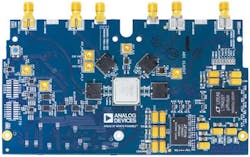
The platform used to demonstrate a real digital filter is Analog Devices’ AD9082 mixed-signal front end (MxFE) (Fig. 1). The data and results from the filter implementations are verified using the platform’s loopback mode connected to a spectrum analyzer.
1. Shown is ADI’s AD9082 MxFE.
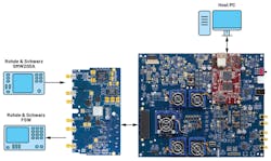
The AD9082 MxFE was set up for testing by interfacing with ADI’s ADS9 development platform to control the analog-to-digital converters (ADCs) and digital-to-analog converters (DACs), and to process the output data. The user guide for this configuration can be found here. A Rohde & Schwarz SMW200A vector signal generator (VSG) was used to generate 5G NR test vectors as well as single and multitone vectors, and an R&S FSW signal and spectrum analyzer was used to measure the output spectrum from the DAC (Fig. 2).
2. The test setup included the AD9082 MxFE, R&S SMW200A vector signal generator, and R&S FSW.
The 192-tap FIR digital filter block (PFILT) is located directly after the ADC cores. To keep things simple, all tests shown in this article are run with one ADC channel being driven single-ended with all 192 taps enabled. The sampling rate of the system was set to 1,500 Msamples/s on both the transmit side and receive side; therefore, all spectra plotted will cover up to Nyquist, or (1500 MHz)/2 = 750 MHz.
Verification Method
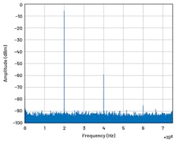
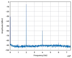
Figures 3 and 4 show a comparison between the ADC data and a spectrum analyzer capture from the DAC outputs using an internal loopback. The spectral representation of these two signals is nearly identical, with a small variation in the noise floor due to the resolution bandwidth of the analyzer. This step was done to confirm that the ADC data after the PFILT matches the output signal from the loopback path.
3. An ADC output of 200 MHz to 5 dBm RFIN.
4. A DAC output of 200 MHz to 5 dBm RFIN.
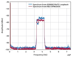
A 5G NR test vector was also used to test the accuracy of indirect loopback by applying a signal with a more complex spectrum. Figure 5 shows the power spectrum of the test vector from the R&S SMW200A VSG compared to the DAC output with loopback.
5. 5G test vectors were compared between the SMW200A output and MxFE DAC output.
Test Results via MATLAB
Filter coefficients for the profiles shown in the results were generated using the MATLAB Filter Designer and retrieved via a Python script that captured trace data from the spectrum analyzer.
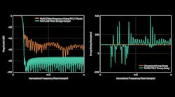
Two plots were generated from each MATLAB Filter Designer output. The first output is the ideal filter profile that shows the digital-filter response, which is possible using a 192-tap FIR filter with double-precision floating-point values. Because the FIR filter takes four hex value codewords as register inputs, some precision is lost while converting to this format from the double values in MATLAB. The expected effects of the datatype conversion on the filter response are shown using a PFILT model and compared to the MATLAB Filter Designer output (Fig. 6 and Table 1).
6. A MATLAB-generated low-pass magnitude response and group delay compared to implemented filter response in an MxFE PFILT model.
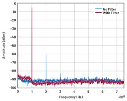
Figure 7 shows the results of a 100-MHz test tone-filtered and looped back to the DAC of the MxFE. The harmonics generated by nonlinearities in the ADC buffers have been filtered by the PFILT, bringing the spurious-free dynamic range (SFDR) from 55.9 dB to 81.9 dB. The implemented filter shows a slower roll-off to 60-dB attenuation than the simulated filter. The group delay was shown to remain flat in the pass band at (N-1)/2 = 95.5 samples for 192 taps.
7. Filtered and nonfiltered DAC output are compared.
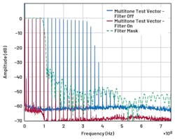
A multitone test vector was generated using the R&S SMW200A (Figs. 8 and 9, and Table 2). This train of tones will conform to the shape of a filter over a broad range of frequencies. The power level of each tone was kept to approximately –40 dBm to avoid intermodulation distortion. As such, the DAC output response with and without filtering is shown with a reference level of –40 dBm.
8. A comparison of multitone test vector MxFE DAC outputs with and without filtering, and a comparison to a MATLAB-generated filter mask. Reference level is –40 dBm.
9. A MATLAB-generated bandpass magnitude response and group delay compared to implemented filter response in an MxFE PFILT model.
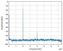
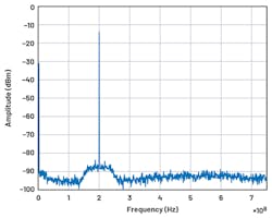
Figures 10 and 11 show a comparison between a 200-MHz CW at –15 dBm. The signal was run through the digital data path and looped back indirectly to the DAC cores. Without the programmable filters active in Figure 10, the harmonic at 2fc measured at –73.88 dBm. With the PFILT active in Figure 11, not only is the harmonic filtered out, but the noise floor of the data path is also reduced and displays the typical Chebyshev out-of-band ripple. In addition, group delay remained flat in the passband for the bandpass filter.
10. An MxFE loopback output with PFILT disabled: 200 MHz to 15 dBm RFIN.
11. An MxFE loopback output with PFILT enabled: 200 MHz to 15 dBm RFIN.
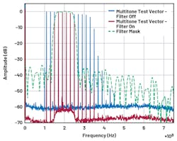
Finally, Figure 12 reveals the results of the bandpass filter applied to the DAC outputs using the same multitone test vector. The passband increases the noise floor by 4.2 dB. However, it reduces the noise floor in the stopband by 2 to 3 dB following the common Chebyshev out-of-band ripple.
12. A multitone test vector MxFE DAC outputs are compared with and without filtering, and compared to MATLAB-generated filter mask. Reference level is –40 dBm.
Latency of the MxFE
Latency through the loopback configuration was measured using a hardware test bench with equal-length coax cables. Total latency measured was 500 ns.
Tables 3 and 4 show the expected latency for the configuration in which the AD9082 was run. The sum of ADC and DAC rates gives minimum to maximum value—500 ns is observed to lie within this range.
Keeping the propagation delay in wireless systems below 1 µs is adequate for ensuring negligible impact on overall network latency and maintaining coherency between link partners. This can apply to 802.11b/g, 4G LTE, and even 5G NR cellphone synchronization. Therefore, demonstrating a latency of 500 ns ensures that even with digital filter delay, the system remains interoperable as a wireless receiver platform for your designs.
Ensuring Accurate and Reliable Data
RF signal chains perform the necessary analog processing to get your signal from waves to bits. However, hardware-side issues like parasitics and power-amplifier nonlinearities, as well as wireless challenges like multipathing and fading, degrade the quality of the signal and turn the signal chain into a nonideal transfer function.
Compensating for attenuation and spectral losses is an important step to ensure your data is accurate and reliable. Using the AD9082 MxFE with programmable filtering gives users the ability to easily design and implement useful filter profiles with sharp transition bands over a wide range of frequencies.
References
“Evaluating the AD9082/AD9081/AD9986/AD9988 Mixed-Signal Front-End (MxFE) RF Transceiver,” Analog Devices Inc., January 2022.
“AD9081/AD9082 System Development User Guide UG-1578,” Analog Devices Inc., July 2021.
“Mixed Signal: Section 6,” Analog Devices Inc.
