This file type includes high resolution graphics and schematics when applicable.
Low-noise amplifiers (LNAs) for high-frequency applications have been based on GaAs metal-epitaxial-semiconductor field-effect-transistor (MESFET) and depletion-mode pseudomorphic-high-electron-mobility-transistor (pHEMT) technologies for some time. Semiconductor technologies such as GaAs heterojunction-bipolar-transistor (HBT) and the newer enhancement-mode pHEMT (E-pHEMT) technologies have been used primarily for power-amplifier (PA) applications. Still, the many outstanding characteristics of E-pHEMT devices also make them suitable for use in high-frequency LNAs capable of wide frequency coverage, including a 100-to-500-MHz LNA which will be revealed here.
For PAs, the performance of E-pHEMT technology offers many well-suited characteristics, including:
- Saturated drain-source current(Idss) of less than 10 µA at room temperature.
- Drain current (Id) of approximately 0 at a gate-source voltage (Vgs) of 0.
- Quiescent drain current (Idq) of less than 30 mA in code-division-multiple-access (CDMA) communications applications.
- Superior output power (Pout) and high efficiency with bias voltages of less than +3 VDC.
- No thermal runaway effects (common to bipolar transistors).
- No secondary breakdown mechanism.
- The ability to survive under high mismatch conditions.
However, E-pHEMT technology can also provide a combination of high gain, low noise, and wide dynamic range in high-linearity LNA applications, such as intermediate-frequency (IF) amplifiers for commercial communication systems and preamplifiers for magnetic-resonance-imaging (MRI) systems. These types of applications have been made practical with the availability of low-cost plastic-packaged surface-mount E-pHEMT devices specifically designed for LNA applications. This article demonstrates why E-pHEMT technology can economically provide superior electrical performance in the VHF and UHF wireless communications bands commonly associated with other technologies, such as GaAs MESFETs and depletion-mode pHEMTs.
The goal of the design project is to produce a 100-to-500-MHz LNA with an output third-order intercept point (OIP3) of +36 dBm, a noise figure below 2.0 dB, and gain of 20 dB with flat gain response. Resistive-capacitive (RC) feedback was used to provide good input and output impedance matching to the active device and to ensure unconditional stability. The matching was also required to reduce the overall stage gain to the specified 20 dB level and maintain flat gain across the 400-MHz operating bandwidth. The amplifier design specification includes operation from a +5-VDC supply with current consumption of less than 65 mA.
The ATF-54143 from Agilent Technologies (San Jose, CA) was selected as the active device for the 100-to-500-MHz LNA. The ATF-54143 is one of a family of high-dynamic-range, low-noise enhancement-mode PHEMT discrete transistors designed for use in low-cost commercial applications in the VHF through 6 GHz frequency range. It is housed in a four-lead SC-70 (SOT-343) surface-mount plastic package and operates from a single regulated supply. If an active bias is desirable for repeatability of the bias setting—particularly desirable in high-volume production—the ATF-54143 requires only the addition of a single PNP bipolar junction transistor. Compared to amplifiers using depletion mode devices, the E-pHEMT design has a lower part count and a more compact layout. Besides having a very low typical noise figure (0.5 dB) at 2 GHz, the ATF-54143 is specified at 2 GHz and +3-VDC bias to provides a +36 dBm output third-order intercept point at 60 mA drain current. A data sheet for this device may be downloaded from: http://literature.agilent.com/litweb/pdf/5989-0034EN.pdf
Using the Advanced Design System (ADS) suite of computer-aided-engineering (CAE) software simulation and analysis tools from Agilent/EEsof (Santa Rosa, CA), the amplifier circuit can be simulated in both linear and nonlinear modes of operation. For the linear analysis, transistors can be modeled with a two-port S-parameter file using the Touchstone format. More information about Agilent electronic-design-automation (EDA) software may be found at: http://www.agilent.com/eesof-eda .The appropriate ATF54143.s2p file can be downloaded from the Agilent Wireless Design Center website:
http://www.semiconductor.agilent.com (type ATF-54143 in the Quick Search at the top of the page. Under Search Results click on the underlined ATF-54143. Scroll down to the S-parameters listing for 60 mA).
For the nonlinear analysis, a harmonic−balance (HB) simulation was used. The HB simulation was preferred over other nonlinear methods because it is computationally fast, handles both distributed and lumped-element circuitry, and can easily include higher-order harmonics and intermodulation products. The HB approach was used for the simulation of the 1-dB compression point (P-1dB) and OIP3.
Although this nonlinear transistor model closely predicts the DC and small-signal behavior (including noise), it does not correctly predict the intercept point. To properly model the exceptionally high linearity of the E-pHEMT transistor, a better model was required.
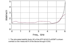
Besides providing information regarding gain, P-1dB, noise figure, and input and output return loss, the simulation provides very important information regarding circuit stability. Unless a circuit is actually oscillating on the bench, it may be difficult to predict instabilities without actually presenting various VSWR loads at various phase angles to the amplifier. Calculating the Rollett stability factor (K) and generating stability circles are two methods made considerably easier with computer simulations. Simulated and measured results show the stability factor, K > 1 (Fig. 1), at the cost of reduced third-order intercept point and output power, through the use of a series resistor on the output.
To meet the goals for noise figure, intercept point and gain, the drain source current (Ids) was chosen to be 60 mA. The characterization data in the device data sheet shows that 60 mA gives the best IP3 combined with a very low minimum noise figure (Fmin). Also, as shown in the data sheet, a 3-V drain-to-source voltage (Vds) gives a slightly higher gain and easily allows the use of a regulated +5-VDC supply.
The use of a controlled amount of source inductance—usually only a few tenths of a nanohenry—can often be used to enhance LNA performance. This is effectively equivalent to increasing the source leads by approximately 0.025 inch or so. The effect can be easily modeled using an RF simulation tool such as ADS. The usual side effect of excessive source inductance is gain peaking at a high frequency and resultant oscillations.
Page Title
Using Active Bias
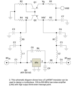
The main advantage of an active biasing scheme is the ability to hold the drain to source current constant over a wide range of temperature variations. A very inexpensive method of accomplishing this is to use two PNP bipolar transistors arranged in a current mirror configuration as shown in Fig. 2.
Due to resistors R1 and R3, this circuit is not a true current mirror, but if the voltage drops across R1 and R3 are kept identical, the current through R3 is stabilized and therefore Ids and Vds are also kept stable. (Note that more information on passive bias networks can be found in Application Note 1222 from Agilent Technologies, at http://literature.agilent.com/litweb/pdf/5988-2336EN.pdf.)
Transistor Q1 is configured with its base and collector tied together. It acts as a simple PN junction, which helps to temperature compensate the emitter-base junction of Q2. To calculate the values of R1, R2, R3, and R4 the following parameters must be known or chosen:
Ids = the device drain-to-source current = 60 mA.
IR = the reference current for active bias = 2.1 mA.
Vdd = is the power supply voltage = +5 VDC;
Vds = the device drain-to-source voltage = +3 VDC;
Vds' = the value of drain-source voltage used in the equations due to the voltage drop across R7 and R8 = +3.56 VDC;
Vgs = the typical gate bias = 0.59 V; and
Vbe1 = the typical base-emitter turn-on voltage for transistors Q1 and Q2 = 0.65 V.
Therefore, resistor R3, which sets the desired device drain current, is calculated as follows:
where:
IC2 is chosen for stability to be 2.1 mA. This value is also equal to the reference current IR.
The next three equations are used to calculate the rest of the biasing resistors for Fig. 1.
Note that the voltage drop across R1 must be set equal to voltage drop across R3, but with a current of IR:
Resistor R2 sets the bias current through Q1:
Resistor R4 sets the gate voltage. Ic2 = Ie2 assuming the hfe of the PNP transistors is high. Calculated resistor values differ from actual resistors due to available component values.
Thus, by forcing the emitter voltage (VE) of transistor Q1 equal to Vds, this circuit regulates the drain current in a manner similar to a current mirror. As long as transistor Q2 operates in the forward active mode, this hold true. In other words the collector-base junction of transistor Q2 must be kept reversed biased.
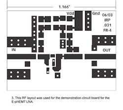
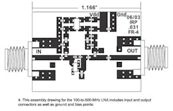
An evaluation board was designed for the feedback amplifier network. This single-layer board (see Figs. 3 and 4) is 0.031-in.-thick FR-4 circuit-board material with a dielectric constant of 4.2.
The feedback network should be made as short as possible, since introducing inductance into the feedback network will cause instability in the 5-to-6-GHz region. The RC feedback uses 40 × 20 mil components that are soldered close together with a small solder pad in between.
The ATF-54143 is conditionally stable below 3.5 GHz, having 29-to-26-dB gain in the 100-to-500-MHz region. The R-C feedback reduces low frequency gain and increases the stability factor to greater than 1 below 2 GHz. The amplifier uses a highpass impedance-matching network, consisting of C1 and L1, for the noise match. The circuit loss will directly relate to noise figure, thus the Q of L1 is extremely important. The LL1608-FSR15 coil from Toko is a small multilayer chip inductor with a rated Q of 19 at 50 MHz. The shunt inductor (L1) provides low frequency gain reduction, which can minimize the amplifier's susceptibility to overload from nearby low-frequency transmitters; it is also part of the input matching network along with C1. Capacitor C1 also doubles as a DC block, while inductor L1 also provides a means of inserting gate voltage for the PHEMT. This requires a good bypass capacitor in the form of C2.
This network represents a compromise between noise figure, input return loss, and gain. Capacitors C2 and C5 provide in-band stability while resistors R5 and R7 provide low-frequency stability by providing a resistive termination. The highpass network on the output consists of a series capacitor C4 and shunt inductors L2, with L2 also providing a means of inserting drain voltage for biasing up the PHEMT. Very short transmission lines between each source lead and ground have been used. The RC-feedback has a dramatic effect on in-band and out-of-band gain, stability, and input and output return loss.
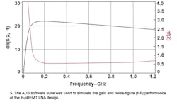
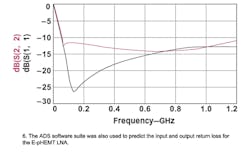
Results from the simulation of gain, NF and for input and output return loss are shown in Figs. 5 and 6, respectively.
- The stimulated stability factor (K) of the ATF-54143 E-pHEMT is shown overlaid on the measured K of the device through 6 GHz.
- This schematic diagram shows how a E-pHEMT transistor can be used to design a multioctave, 100-to-500-MHz low-noise amplifier (LNA) with high output third-order intercept point.
- This RF layout was used for the demonstration circuit board for the E-pHEMT LNA.
- This assembly drawing for the 100-to-500-MHz LNA includes input and output connectors as well as ground and bias points.
- The ADS software suite was used to simulate the gain and noise-figure (NF) performance of the E-pHEMT LNA design.
- The ADS software suite was also used to predict the input and output return loss for the E-pHEMT LNA.
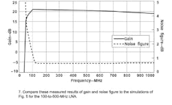
- Compare these measured results of gain and noise figure to the simulations of Fig. 5 for the 100-to-500-MHz LNA.
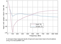
- Compare these measured results of input and output return loss to the simulations of Fig. 6 for the E-pHEMT LNA.
This file type includes high resolution graphics and schematics when applicable.


